Vista de Lectura

Hay nuevos artículos disponibles. Pincha para refrescar la página.

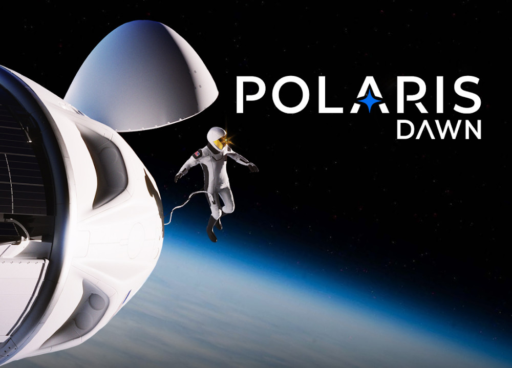
Polaris Dawn, and the Prudence of a Short Spacewalk

For months before liftoff, the popular press had been hyping up the fact that the Polaris Dawn mission would include the first-ever private spacewalk. Not only would this be the first time anyone who wasn’t a professional astronaut would be opening the hatch of their spacecraft and venturing outside, but it would also be the first real-world test of SpaceX’s own extravehicular activity (EVA) suits. Whether you considered it a billionaire’s publicity stunt or an important step forward for commercial spaceflight, one thing was undeniable: when that hatch opened, it was going to be a moment for the history books.

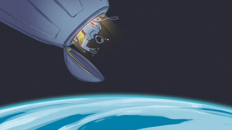
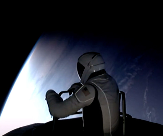
But if you happened to have been watching the live stream of the big event earlier this month, you’d be forgiven for finding the whole thing a bit…abrupt. After years of training and hundreds of millions of dollars spent, crew members Jared Isaacman and Sarah Gillis both spent less than eight minutes outside of the Dragon capsule. Even then, you could argue that calling it a spacewalk would be a bit of a stretch.

Neither crew member ever fully exited the spacecraft, they simply stuck their upper bodies out into space while keeping their legs within the hatch at all times. When it was all said and done, the Dragon’s hatch was locked up tight less than half an hour after it was opened.

Likely, many armchair astronauts watching at home found the whole thing rather anticlimactic. But those who know a bit about the history of human spaceflight probably found themselves unable to move off of the edge of their seat until that hatch locked into place and all crew members were back in their seats.

Flying into space is already one of the most mindbogglingly dangerous activities a human could engage in, but opening the hatch and floating out into the infinite black once you’re out there is even riskier still. Thankfully the Polaris Dawn EVA appeared to go off without a hitch, but not everyone has been so lucky on their first trip outside the capsule.

A High Pressure Situation

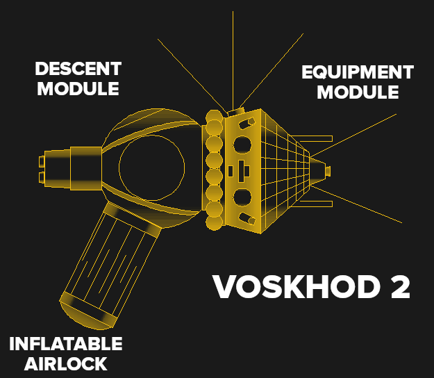
The first-ever EVA took place during the Voskhod 2 mission in March of 1965. Through the use of an ingenious inflatable airlock module, cosmonaut Alexei Leonov was able to exit the Voskhod 3KD spacecraft and float freely in space at the end of a 5.35 m (17.6 ft) tether. He attached a camera to the outside of the airlock, providing a visual record of yet another space “first” achieved by the Soviet Union.

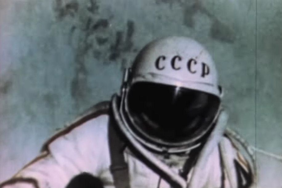
This very first EVA had two mission objectives, one of which Leonov had accomplished when he successfully rigged the external camera. The last thing he had to do was turn around and take pictures of the Voskhod spacecraft flying over the Earth — a powerful propaganda image that the USSR was eager to get their hands on. But when he tried to activate his suit’s camera using the trigger mounted to his thigh, he found he couldn’t reach it. It was then that he realized the suit had begun to balloon around him, and that moving his arms and legs was taking greater and greater effort due to the suit’s material stiffening.

After about ten minutes in space Leonov attempted to re-enter the airlock, but to his horror found that the suit had expanded to the point that it would no longer fit into the opening. As he struggled to cram himself into the airlock, his body temperature started to climb. Soon he was sweating profusely, which pooled around his body within the confines of the suit.

Unable to cope with the higher than anticipated internal temperature, the suit’s primitive life support system started to fail, making matters even worse. The runaway conditions in the suit caused his helmet’s visor to fog up, which he had no way to clear as he was now deep into a failure mode that the Soviet engineers had simply not anticipated. Not that they hadn’t provided him with a solution of sorts. Decades later, Leonov would reveal that there was a suicide pill in the helmet that he could have opted to use if need be.

With his core temperature now elevated by several degrees, Leonov was on the verge of heat stroke. His last option was to open a vent in his suit, which would hopefully cause it to deflate enough for him to fit inside the airlock. He noted that the suit was currently at 0.4 atmosphere, and started reducing the pressure. The safety minimum was 0.27 atm, but even at that pressure, he couldn’t fit. It wasn’t until the pressure fell to 0.25 atm that he was able to flex the suit enough to get his body back into the airlock, and from there back into the confines of the spacecraft.

In total, Alexei Leonov spent 12 minutes and 9 seconds in space. But it must have felt like an eternity.

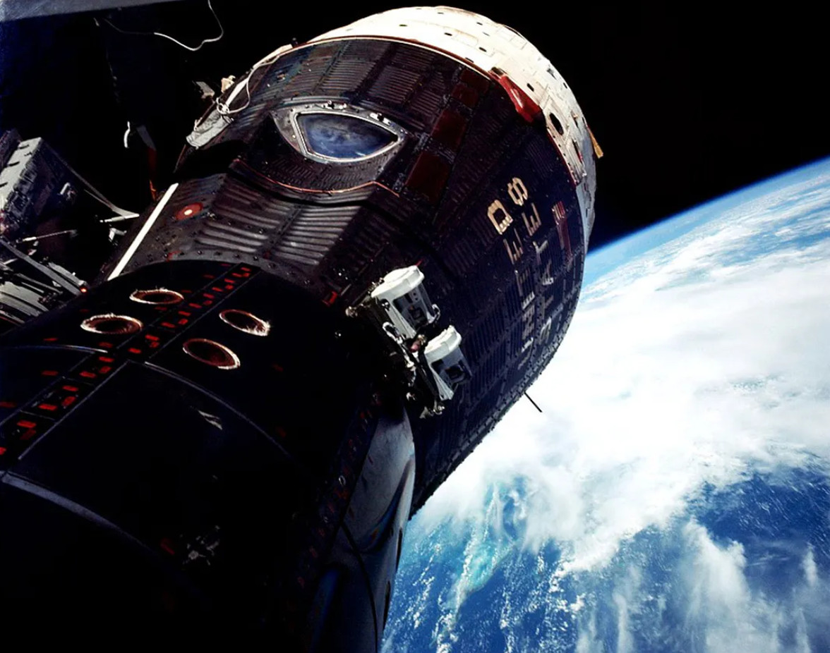
Gemini’s Tricky Hatch

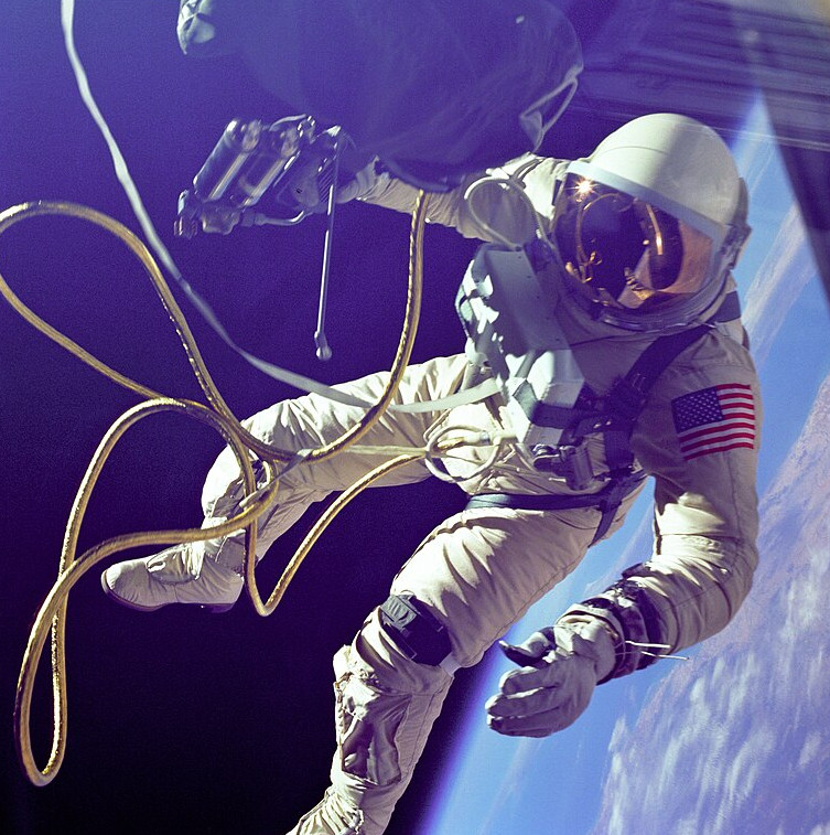
In classic Soviet style, nobody would know about the trouble Leonov ran into during his spacewalk for years. So when American astronaut Ed White was preparing to step out of the Gemini 4 capsule three months later in June of 1965, he believed he really had his work cut out for him. Not only had the Soviets pulled off a perfect EVA, but as far as anyone knew, they had made it look easy.

So it’s not hard to imagine how White must have felt when he pulled the lever to open the hatch on the Gemini spacecraft, only to find it refused to budge. As it so happens, this wasn’t the first time the hatch failed to open. During vacuum chamber testing back on the ground, the hatch had refused to lock because a spring-loaded gear in the mechanism failed to engage properly. Luckily the second astronaut aboard the Gemini capsule, James McDivitt, was present when they had this issue on the ground and knew how the latch mechanism functioned.

Ed White

McDivitt felt confident that he could get the gear to engage and allow White to open the hatch, but was concerned about getting it closed. Failing to open the hatch and calling off the EVA was one thing, but not being able to secure the hatch afterwards meant certain death for the two men. Knowing that Mission Control would almost certainly have told them to abort the EVA if they were informed about the hatch situation, the astronauts decided to go ahead with the attempt.

As he predicted, McDivitt was able to fiddle with the latching mechanism and got the hatch open for White. Although there were some communication issues during the spacewalk due to problems with the voice-operated microphones, the EVA went very well, with White demonstrating a hand-held maneuvering thruster that allowed him to fly around the spacecraft at the end of his tether.

White was having such a good time that he kept making excuses to extend the spacewalk. Finally, after approximately 23 minutes, he begrudgingly returned to the Gemini capsule — informing Mission Control that it was “the saddest moment of my life.”

The hatch had remained open during the EVA, but now that White was strapped back into the capsule, it was time to close it back up. Unfortunately, just as McDivitt feared, the latches wouldn’t engage. To make matters worse, it took White so long to get back into the spacecraft that they were now shadowed by the Earth and working in the dark. Reaching blindly inside the mechanism, White was once again able to coax it into engaging, and the hatch was securely closed.

But there was still a problem. The mission plan called for the astronauts to open the hatch so they could discard unnecessary equipment before attempting to reenter the Earth’s atmosphere. As neither man was willing to risk opening the hatch again, they instead elected to stow everything aboard the capsule for the remainder of the flight.

Overworked, and Underprepared

At this point the Soviet Union and the United States had successfully conducted EVAs, but both had come dangerously close to disaster. Unfortunately, between the secretive nature of the Soviets and the reluctance of the Gemini 4 crew to communicate their issues to Mission Control, NASA administration started to underestimate the difficulties involved.

NASA didn’t even schedule EVAs for the next three Gemini missions, and the ambitious spacewalk planned for Gemini 8 never happened due to the mission being cut short due to technical issues with the spacecraft. It wouldn’t be until Gemini 9A that another human stepped out of their spacecraft.

The plan was for astronaut Gene Cernan to spend an incredible two hours outside of the capsule, during which time he would make his way to the rear of the spacecraft where a prototype Astronaut Maneuvering Unit (AMU) was stored. Once there, Cernan was to disconnect himself from the Gemini tether and don the AMU, which was essentially a small self-contained spacecraft in its own right.

Photo of the Gemini spacecraft taken by Gene Cernan

But as soon as he left the capsule, Cernan reported that his suit had started to swell and that movement was becoming difficult. To make matters worse, there were insufficient handholds installed on the outside of the Gemini spacecraft, making it difficult for him to navigate his away along its exterior. After eventually reaching the AMU and struggling desperately to put it on, Mission Control noted his heart rate had climbed to 180 beats per minute. The flight surgeon was worried he would pass out, so Mission Control asked him to take a break while they debated if he should continue with the AMU demonstration.

At this point Cernan noted that his helmet’s visor had begun to fog up, and just as Alexei Leonov had discovered during his own EVA, the suit had no system to clear it up. The only way he was able to see was by stretching forward and clearing off a small section of the glass by rubbing his nose against it. Realizing the futility of continuing, Commander Thomas Stafford decided not to wait on Mission Control and ordered Cernan to abort the EVA and get back into the spacecraft.

Cernan slowly made his way back to the Gemini’s hatch. The cooling system in his suit had by now been completely overwhelmed, which caused the visor to fog up completely. Effectively blind, Cernan finally arrived at the spacecraft’s hatch, but was too exhausted to continue. Stafford held onto Cernan’s legs while he rested and finally regained the strength to lower himself into the capsule and close the hatch.

When they returned to Earth the next day, a medical examination revealed Cernan had lost 13 pounds (5.8 kg) during his ordeal. The close-call during his spacewalk lead NASA to completely reassess their EVA training and procedures, and the decision was made to limit the workload on all future Gemini spacewalks, as the current air-cooled suit clearly wasn’t suitable for long duration use. It wasn’t until the Apollo program introduced a liquid-cooled suit that American astronauts would spend any significant time working outside of their spacecraft.

The Next Giant Leap

Thanks to the magic of live streaming video, we know that the Polaris Dawn crew was able to complete their brief EVA without incident: no shadowy government cover-ups, cowboy heroics, or near death experiences involved.

With the benefit of improved materials and technology, not to mention the knowledge gained over the hundreds of spacewalks that have been completed since the early days of the Space Race, the first private spacewalk looked almost mundane in comparison to what had come before it.

But there’s still much work to be done. SpaceX needs to perform further tests of their new EVA suit, and will likely want to demonstrate that crew members can actually get work done while outside of the Dragon. So it’s safe to assume that when the next Polaris Dawn mission flies, its crew will do a bit more than just stick their heads out the hatch.

Pi Zero Power Optimization Leaves No Stone Unturned

If you’ve ever designed a battery-powered device with a Pi Zero, you have no doubt looked into decreasing its power consumption. Generic advice, like disabling the HDMI interface and the onboard LED, is omnipresent, but [Manawyrm] from [Kittenlabs] goes beyond the surface-level, and gifts us an extensive write-up where every recommendation is backed with measurements. Armed with the Nordic Power Profiler kit and an SD card mux for quick experimentation, she aimed at two factors, boot time and power consumed while booting, and made sure to get all the debug information we could use.

Thanks to fast experimentation cycles and immediate feedback, we learn plenty of new things about what a Pi Zero does and when, and how we can tame various power-hungry aspects of its behavior. Disabling the GPU or its aspects like HDMI output, tweaking features like HAT and other peripheral probing, and even tactical overclocking during boot – it’s an extensive look at what makes a Pi Zero tick, and no chance for spreading baseless advice or myths.

All in all, this write-up helps you decrease the boot time from twelve seconds to just three seconds, and slash the power budget of the boot process by 80%. Some recommendations are as simple as config.txt entries, while others require you to recompile the kernel. No matter the amount of effort you can put into power optimization, you’ll certainly find things worth learning while following along, and [Manawyrm]’s effort in building her solar-powered Pi setup will help us all build better Pi-Zero-powered solar devices and handhelds.

The 1924 Martian Signal: A Cosmic Curiosity

Visual of sound against a dark red sky

In an age where our gadgets allow us to explore the cosmos, we stumbled upon sounds from a future past: an article on historical signals from Mars. The piece, written by [Paul Gilster] of Centauri Dreams, cites a Times essay published by [Becky Ferreira] of August 20. [Ferreira]’s essay sheds light on a fascinating, if peculiar, chapter in the history of the search for extraterrestrial life.

She recounts an event from August 1924 when the U.S. Navy imposed a nationwide radio silence for five minutes each hour to allow observatories to listen for signals from Mars. This initiative aimed to capitalize on the planet’s close alignment with Earth, sparking intrigue and excitement among astronomers and enthusiasts alike.

Amid the technological optimism of the era, a dirigible equipped with radio equipment took to the skies to monitor potential Martian messages. The excitement peaked when a series of dots and dashes captured by the airborne antenna suggested a “crudely drawn face.” Some scientists speculated that this could be a signal from a Martian civilization, igniting a media frenzy. Yet, skeptics, including inventor C. Francis Jenkins, suggested these results were merely a case of radio frequency interference—an early reminder of the challenges we face in discerning genuine signals from the noise of our own planet.

As we tinker with our devices and dream of interstellar communication, the 1924 incident reminds us that the search for extraterrestrial intelligence is a blend of curiosity, creativity, and, often, misinterpretation.

Laptop GPU Upgrade With Just A Little Reballing

Modern gaming laptops are in an uncomfortable spot – often too underpowered for newest titles, but too bulky to be genuinely portable. It doesn’t help they’re not often upgradeable, so you’re stuck with what you’ve bought – unless, say, you’re a hacker equipped some tools for PCB reflow? If that’s the case, welcome to [TechModLab]’s video showing you the process of upgrading a laptop’s soldered-on NVIDIA GPU, replacing the 3070 chip with a 3080.

You don’t need much – the most exotic tool is a BGA rework station, holding the mainboard steady&stiff and heating a specific large chip on the board with an infrared lamp from above. This one is definitely a specialty tool, but we’ve seen hackers build their own. From there, some general soldering tools like flux and solder wick, a stencil for your chip, BGA balls, and a $20 USB-C hotplate are instrumental for reballing chips – tools you ought to have.

Reballing was perhaps the hardest step of the journey – instrumental for preparing the GPU before the transplant. Afterwards, only a few steps were needed – poking a BGA ball that didn’t connect, changing board straps to adjust for the new VRAM our enterprising hacker added alongside the upgrade, and playing with the driver process install a little. Use this method to upgrade from a lower-end binned GPU you’re stuck with, or perhaps to repair your laptop if artifacts start appearing – it’s a worthwhile reminder about methods that laptop repair shops use on the daily.

Itching to learn more about BGAs? You absolutely should read this article series by our own [Robin Kearey]. We’ve mostly seen reballing used for upgrading RAM on laptop and Raspberry Pi boards, but seeing it being used for an entire laptop is nice – it’s the same technique, just scaled up, and you always can start by practicing at a smaller scale. Now, it might feel like we’ve left the era of upgradable GPUs on laptops, and today’s project might not necessarily help your worries – but the Framework 16 definitely bucks the trend.

Voyager 2’s Plasma Spectrometer Turned Off in Power-Saving Measure

The Voyager 2 spacecraft’s energy budget keeps dropping by about 4 Watt/year, as the plutonium in its nuclear power source is steadily dropping as the isotope decays. With 4 Watt of power less to use by its systems per year, the decision was made to disable the plasma spectrometer (PLS) instrument. As also noted by the NASA Voyager 2 team on Twitter, this doesn’t leave the spacecraft completely blind to plasma in the interstellar medium as the plasma wave subsystem (PWS) is still active. The PLS was instrumental in determining in 2018 that Voyager 2 had in fact left the heliosphere and entered interstellar space. The PLS on Voyager 1 had already broken down in 1980 and was turned off in 2007.

After saving the Voyager 1 spacecraft the past months from a dud memory chip and switching between increasingly clogged up thrusters, it was now Voyager 2’s turn for a reminder of the relentless march of time and the encroaching end of the Voyager missions. Currently Voyager 2 still has four active instruments, but by the time the power runs out, they’ll both be limping along with a single instrument, probably somewhere in the 2030s if their incredible luck holds.

This incredible feat was enabled both by the hard work and brilliance of the generations of teams behind the two spacecraft, who keep coming up with new tricks to save power, and the simplicity of the radioisotope generators (RTGs) which keep both Voyagers powered and warm even in the depths of interstellar space.

MikroPhone – Open, Secure, Simple Smartphone

Modern smartphones try and provide a number of useful features to their users, and yet, they’re not exactly designed with human needs in mind. A store-bought smartphone will force a number of paradigms and features onto you no matter whether you want them, and, to top it off, it will encroach on your privacy and sell your data. It’s why self-built and hacker-friendly smartphone projects keep popping up, and the MikroPhone project fills a new niche for sure, with its LTE connectivity making it a promising option for all hackers frustrated with the utter state of smartphones today.

MikroPhone is open-source in every single aspect possible, and it’s designed to be privacy-friendly and easy to understand. At its core is a SiFive Freedom E310, a powerful RISC-V microcontroller – allowing for a feature phone-like OS that is easy to audit and hard to get bogged down by. You’re not limited to a feature phone OS, however – on the PCB, you will find a slot for an NXP i.MX8M-based module that can run a Linux-based mobile OS of your choice. MikroPhone’s display and touchscreen are shared between the Linux module and the onboard MCU, a trick that reminds us of the MCH2022 badge – you get as much “smartphone” as you currently need, no more, no less.

The cool features at MikroPhone’s core don’t end here. The MikroPhone has support for end-to-end encrypted communications, kept to its feature-phone layer, making for a high bar of privacy protection – even when the higher-power module might run an OS that you don’t necessarily fully trust. Currently, MikroPhone is a development platform, resembling the PinePhone’s Project Don’t Be Evil board back when PinePhone was just starting out, and just like with PinePhone, it wouldn’t be hard to minify this platform into a pocket-friendly form-factor, either. The PinePhone has famously become a decent smartphone replacement option in the hacker world, even helping kick off a few mobile OS projects and resulting in a trove of hacks to grace our pages.

Witch’s Staff Build is a Rad Glowing Costume Prop

Let’s say you’re going to a music festival. You could just take water, sunscreen, and a hat. Or, you could take a rad glowing witch’s staff to really draw some eyes and have some fun. [MZandtheRaspberryPi] recently undertook just such a build for a friend and we love how it turned out.

The concept was to build a staff or cane with a big glowing orb on top. The aim was to 3D print the top as a very thin part so that LEDs inside could glow through it. Eventually, after much trial and error, the right combination of design and printer settings made this idea work. A Pi Pico W was then employed as the brains of the operation, driving a number of through-hole Neopixel LEDs sourced from Adafruit.

Power was courtesy of a long cable running out of the cane and to a USB power bank in the wielder’s pocket. Eventually, it was revealed this wasn’t ideal for dancing with the staff. Thus, an upgrade came in the form of an Adafruit Feather microcontroller and a 2,000 mAh lithium-polymer battery tucked inside the orb. The Feather’s onboard hardware made managing the lithium cell a cinch, and there were no more long cables to worry about.

The result? A neat costume prop that looks fantastic. A bit of 3D printing and basic electronics is all you need these days to build fun glowing projects, and we always love to see them. Halloween is right around the corner — if you’re building something awesome for your costume, don’t hesitate to let us know!

Mining and Refining: Lead, Silver, and Zinc

If you are in need of a lesson on just how much things have changed in the last 60 years, an anecdote from my childhood might suffice. My grandfather was a junk man, augmenting the income from his regular job by collecting scrap metal and selling it to metal recyclers. He knew the current scrap value of every common metal, and his garage and yard were stuffed with barrels of steel shavings, old brake drums and rotors, and miles of copper wire.

But his most valuable scrap was lead, specifically the weights used to balance car wheels, which he’d buy as waste from tire shops. The weights had spring steel clips that had to be removed before the scrap dealers would take them, which my grandfather did by melting them in a big cauldron over a propane burner in the garage. I clearly remember hanging out with him during his “melts,” fascinated by the flames and simmering pools of molten lead, completely unconcerned by the potential danger of the situation.

Fast forward a few too many decades and in an ironic twist I find myself living very close to the place where all that lead probably came from, a place that was also blissfully unconcerned by the toxic consequences of pulling this valuable industrial metal from tunnels burrowed deep into the Bitterroot Mountains. It didn’t help that the lead-bearing ores also happened to be especially rich in other metals including zinc and copper. But the real prize was silver, present in such abundance that the most productive silver mine in the world was once located in a place that is known as “Silver Valley” to this day. Together, these three metals made fortunes for North Idaho, with unfortunate side effects from the mining and refining processes used to win them from the mountains.

All Together Now

Thanks to the relative abundance of their ores and their physical and chemical properties, lead, silver, and zinc have been known and worked since prehistoric times. Lead, in fact, may have been the first metal our ancestors learned to smelt. It’s primarily the low melting points of these metals that made this possible; lead, for instance, melts at only 327°C, well within the range of a simple wood fire. It’s also soft and ductile, making it easy enough to work with simple tools that lead beads and wires dating back over 9,000 years have been found.

Unlike many industrial metals, minerals containing lead, silver, and zinc generally aren’t oxides of the metals. Rather, these three metals are far more likely to combine with sulfur, so their ores are mostly sulfide minerals. For lead, the primary ore is galena or lead (II) sulfide (PbS). Galena is a naturally occurring semiconductor, crystals of which lent their name to the early “crystal radios” which used a lump of galena probed with a fine cat’s whisker as a rectifier or detector for AM radio signals.

Geologically, galena is found in veins within various metamorphic rocks, and in association with a wide variety of sulfide minerals. Exactly what minerals those are depends greatly on the conditions under which the rock formed. Galena crystallized out of low-temperature geological processes is likely to be found in limestone deposits alongside other sulfide minerals such as sphalerite, or zincblende, an ore of zinc. When galena forms under higher temperatures, such as those associated with geothermal processes, it’s more likely to be associated with iron sulfides like pyrite, or Fool’s Gold. Hydrothermal galenas are also more likely to have silver dissolved into the mineral, classifying them as argentiferous ores. In some cases, such as the mines of the Silver Valley, the silver is at high enough concentrations that the lead is considered the byproduct rather than the primary product, despite galena not being a primary ore of silver.

Like a Lead Bubble

How galena is extracted and refined depends on where the deposits are found. In some places, galena deposits are close enough to the surface that open-cast mining techniques can be used. In the Silver Valley, though, and in other locations in North America with commercially significant galena deposits, galena deposits follow deep fissures left by geothermal processes, making deep tunnel mining more likely to be used. The scale of some of the mines in the Silver Valley is hard to grasp. The galena deposits that led to the Bunker Hill stake in the 1880s were found at an elevation of 3,600′ (1,100 meters) above sea level; the shafts and workings of the Bunker Hill Mine are now 1,600′ (488 meters) below sea level, requiring miners to take an elevator ride one mile straight down to get to work.

Ore veins are followed into the rock using a series of tunnels or stopes that branch out from vertical shafts. Stopes are cut with the time-honored combination of drilling and blasting, freeing up hundreds of tons of ore with each blasting operation. Loose ore is gathered with a slusher, a bucket attached to a dragline that pulls ore back up the stope, or using mining loaders, low-slung payloaders specialized for operation in tight spaces.

Ore plus soap equals metal bubbles. Froth flotation of copper sulfide is similar to the process for extracting zinc sulfide. Source: Geomartin, CC BY-SA 4.0

Silver Valley galena typically assays at about 10% lead, making it a fairly rich ore. It’s still not rich enough, though, and needs to be concentrated before smelting. Most mines do the initial concentration on site, starting with the usual crushing, classifying, washing, and grinding steps. Ball mills are used to reduce the ore to a fine powder, mixed with water and surfactants to form a slurry, and pumped into a broad, shallow tank. Air pumped into the bottom of the tanks creates bubbles in the slurry that carry the fine lead particles up to the surface while letting the waste rock particles, or gangue, sink to the bottom. It seems counterintuitive to separate lead by floating it, but froth flotation is quite common in metal refining; we’ve seen it used to concentrate everything from lightweight graphite to ultradense uranium. It’s also important to note that this is not yet elemental lead, but rather still the lead sulfide that made up the bulk of the galena ore.

Once the froth is skimmed off and dried, it’s about 80% pure lead sulfide and ready for smelting. The Bunker Hill Mine used to have the largest lead smelter in the world, but that closed in 1982 after decades of operation that left an environmental and public health catastrophe in its wake. Now, concentrate is mainly sent to smelters located overseas for final processing, which begins with roasting the lead sulfide in a blast of hot air. This converts the lead sulfide to lead oxide and gaseous sulfur dioxide as a waste product:

2 PbS + 3 O{_2} \rightarrow2 PbO + 2 SO{_2}

After roasting, the lead oxide undergoes a reduction reaction to free up the elemental lead by adding everything to a blast furnace fueled with coke:

2 PbO + C \rightarrow2 Pb + CO{_2}

Any remaining impurities float to the top of the batch while the molten lead is tapped off from the bottom of the furnace.

Zinc!

A significant amount of zinc is also located in the ore veins of the Silver Valey, enough to become a major contributor to the district’s riches. The mineral sphalerite is the main zinc ore found in this region; like galena, it’s a sulfide mineral, but it’s a mixture of zinc sulfide and iron sulfide instead of the more-or-less pure lead oxide in galena. Sphalerite also tends to be relatively rich in industrially important contaminants like cadmium, gallium, germanium, and indium.

Most sphalerite ore isn’t this pretty. Source: Ivar Leidus, CC BY-SA 4.0.

Extraction of sphalerite occurs alongside galena extraction and uses mostly the same mining processes. Concentration also uses the froth flotation method used to isolate lead sulfide, albeit with different surfactants specific for zinc sulfide. Concentration yields a material with about 50% zinc by weight, with iron, sulfur, silicates, and trace metals making up the rest.

Purification of zinc from the concentrate is via a roasting process similar to that used for lead, and results in zinc oxide and more sulfur dioxide:

2 ZnS + 3 O{_2}\rightarrow2 ZnO + 2SO{_2}

Originally, the Bunker Hill smelter just vented the sulfur dioxide out into the atmosphere, resulting in massive environmental damage in the Silver Valley. My neighbor relates his arrival in Idaho in 1970, crossing over the Lookout Pass from Montana on the then brand-new Interstate 90. Descending into the Silver Valley was like “a scene from Dante’s Inferno,” with thick smoke billowing from the smelter’s towering smokestacks trapped in the valley by a persistent inversion. The pine trees on the hillsides had all been stripped of needles by the sulfuric acid created when the sulfur dioxide mixed with moisture in the stale air. Eventually, the company realized that sulfur was too valuable to waste and started capturing it, and even built a fertilizer plant to put it to use. But the damage was done, and it took decades for the area to bounce back.

Recovering metallic zinc from zinc oxide is performed by reduction, again in a coke-fired blast furnace which collects the zinc vapors and condenses them to the liquid phase, which is tapped off into molds to create ingots. An alternative is electrowinning, where zinc oxide is converted to zinc sulfate using sulfuric acid, often made from the sulfur recovered from roasting. The zinc sulfate solution is then electrolyzed, and metallic zinc is recovered from the cathodes, melted, further purified if necessary, and cast into ingots.

Silver from Lead

If the original ore was argentiferous, as most of the Silver Valley’s galena is, now’s the time to recover the silver through the Parke’s process, a solvent extraction technique. In this case, the solvent is the molten lead, in which silver is quite soluble. The dissolved silver is precipitated by adding molten zinc, which has the useful property of reacting with silver while being immiscible with lead. Zinc also has a higher melting point than lead, meaning that as the temperature of the mixture drops, the zinc solidifies, carrying along any silver it combined with while in the molten state. The zinc-silver particles float to the top of the desilvered lead where they can be skimmed off. The zinc, which has a lower boiling point than silver, is driven off by vaporization, leaving behind relatively pure silver.

To further purify the recovered silver, cupellation is often employed. Cupellation is a pyrometallurgical process used since antiquity to purify noble metals by exploiting the different melting points and chemical properties of metals. In this case, silver contaminated with zinc is heated to the point where the zinc oxidizes in a shallow, porous vessel called a cupel. Cupels were traditionally made from bone ash or other materials rich in calcium carbonate, which gradually absorbs the zinc oxide, leaving behind a button of purified silver. Cupellation can also be used to purify silver directly from argentiferous galena ore, by differentially absorbing lead oxide from the molten solution, with the obvious disadvantage of wasting the lead:

Ag + 2 Pb + O{_2}\rightarrow 2PbO + Ag

Cupellation can also be used to recover small amounts of silver directly from refined lead, such as that in wheel weights:

If my grandfather had only known.

Creating Video Games With AI: a Mario Example

Artificial intelligence (AI) seems to be doing everything these days. Making images, making videos, and replacing most of us real human writers if you believe the hype. Maybe it’s all over! And yet, we persist, to write about yet another job taken over by AI: creating video games.

The research paper is entitled “Video Game Generation: A Practical Study using Mario.” The basic idea is whether a generative AI model can create an interactive video game by first training it on an existing game.

MarioVGG, as it is called, is a “text-to-video model.” It hasn’t built the Mario game that you’re familiar with, though. It takes player commands as text inputs—such as “run, or “jump”—and then outputs video frames showing the result in the ‘game.’ The model was trained on a dataset of frame-by-frame Super Mario Brothers game play, combined with data on user inputs at the time. The model shows an ability to generate believable video output for given player inputs, including basic game physics, item interactions, and collisions. It’s able to do this in a chained way, so that it can reasonably simulate a player making multiple actions and moving through a level of the game.

It’s not like playing a real Mario game yet, by any means. Regardless, the AI model has shown an ability to replicate the world of the game in a way that behaves relatively consistently with its established rules. If you’re in the field of video game development, though, you probably don’t have a lot to worry about just yet—you probably moved past making basic Mario clones years ago, so you’ve got quite an edge for now!

Easily Build This IMU Array Sandbox

These days we’re used to our devices containing an inertial measurement unit (IMU) that lets it know its position relative to the Earth. They’re mechanical devices at heart, and so they’re not infallible, with a few well-known failure modes — but we can try and help it. One way that’s getting some attention is to put many MEMS IMUs on a single PCB, connect it to an FPGA, then process their data all together to make for a more sensitive IMU or filter out drift. Want to join in? Here’s an open source implementation from [will127534].

With 32 individual ICM-42688-P SPI-connected IMUs and the beloved ICE40 chip at the center of the board, this PCB is a powerful platform to help you jump onto the new direction of the IMU research world. There’s example Verilog code that tests the board’s workings, and you can pair it with a Pi Pico running MicroPython to test out its raw capabilities. After that, the stage is yours.

The board is cheap to order online, easy to assemble yourself if you must, or have JLCPCB assemble it — just solder some capacitors on the backside afterwards. There’s a breakout, but it’s mostly for tests. This board is very much designed to be a module in a bigger system, [will] mentions that he’s building a geophone. Clever array-based hacks are en vogue, it would feel – here’s a LED array from [mitxela] that uses LEDs as sensors.

BBC Micro: A Retro Revamp with the 68008 Upgrade

Screen caps of upgraded BBC Micro, and OS 9 code

The BBC Microcomputer, launched in the early 1980s, holds a special place in computing history. Designed for educational purposes, it introduced a generation to programming and technology. With its robust architecture and community-driven modifications, the BBC Micro remains a beloved project for retro computing enthusiasts. [Neil] from Retro4U has been delving into this classic machine, showcasing the fascinating process of repairing and upgrading his BBC Micro with a 68008 CPU upgrade.

Last week, [Neil] shared his progress, unveiling advancements in his repairs and upgrades. After tackling a troublesome beep issue, he successfully managed to get the BBC running with 32 KB of functional memory, allowing him to boot into BASIC. But he wasn’t stopping there. With ambitions set on installing the 68008 CPU, [Neil]’s journey continued.

The 68008 board offers significant enhancements, including multitasking capabilities with OS-9 and its own hard drive and floppy disk controller. However, [Neil] quickly encountered challenges; the board’s condition revealed the usual broken capacitors and a few other faulty components. After addressing these issues, [Neil] turned his attention to programming the necessary ROM for OS-9.

Looking to get your hands dirty? [Neil] has shared a PDF of the upgrade circuit diagram. You can also join the discussion with fellow enthusiasts on his Discord channel, linked in the video description.

ROG Ally Community Rebuilds The Proprietary Asus eGPU

As far as impressive hacks go, this one is more than enough for your daily quota. You might remember the ROG Ally, a Steam Deck-like x86 gaming console that’s graced our pages a couple lf times. Now, this is a big one – from the ROG Ally community, we get a fully open-source eGPU adapter for the ROG Ally, built by reverse-engineering the proprietary and overpriced eGPU sold by Asus.

We’ve seen this journey unfold over a year’s time, and the result is glorious – two different PCBs, one of them an upgraded drop-in replacement board for the original eGPU, and another designed to fit a common eGPU form-factor adapter. The connector on the ROG Ally is semi-proprietary, but its cable could be obtained as a repair part. From there, it was a matter of scrupulous pinout reverse-engineering, logic analyzer protocol captures, ACPI and BIOS decompiling, multiple PCB revisions and months of work – what we got is a masterpiece of community effort.

Do you want to learn how the reverse-engineering process has unfolded? Check out the Diary.md – it’s certainly got something for you to learn, especially if you plan to walk a similar path; then, make sure to read up all the other resources on the GitHub, too! This achievement follows a trend from the ROG Ally community, with us having featured dual-screen mods and battery replacements before – if it continues the same way, who knows, maybe next time we will see a BGA replacement or laser fault injection.

Xiaomi M365 Battery Fault? Just Remove A Capacitor

Electric scooters have long been a hacker’s friend, Xiaomi ones in particular – starting with M365, the Xiaomi scooter family has expanded a fair bit. They do have a weak spot, like many other devices – the battery, something you expect to wear out.

Let’s say, one day the scooter’s diagnostics app shows one section of the battery going way below 3 volts. Was it a sudden failure of one of the cells that brought the whole stage down? Or perhaps, water damage after a hastily assembled scooter? Now, what if you measure the stages with a multimeter and it turns out they are perfectly fine?

Turns out, it might just be a single capacitor’s fault. In a YouTube video, [darieee] tells us all about debugging a Xiaomi M365 battery with such a fault – a BQ76930 controller being responsible for measuring battery voltages. The BMS (Battery Management System) board has capacitors in parallel with the cells, and it appears that some of these capacitors can go faulty.

Are you experiencing this particular fault? It’s easy to check – measure the battery stages and see if the information checks out with the readings in your scooter monitoring app of choice. Could this be a mechanical failure mode for this poor MLCC? Or maybe, a bad batch of capacitors? One thing is clear, this case is worth learning from, adding this kind of failure to your collection of fun LiIon pack tidbits. This pack seems pretty hacker-friendly – other packs lock up when anything is amiss, like the Ryobi batteries do, overdue for someone to really spill their secrets!

Print Yourself Penrose Wave Tiles As An Excellent Conversation Starter

Ah, tiles. You can get square ones, and do a grid, or you can get fancier shapes and do something altogether more complex. By and large though, whatever pattern you choose, it will normally end up repeating on some scale or other. That is, unless you go with something like a Penrose Wave Tile. Discovered by mathematician Roger Penrose, they never exactly repeat, no matter how you lay them out.

[carterhoefling14] decided to try and create Penrose tiles at home—with a 3D printer being the perfect route to do it. Creating the tiles was simple—the first step was to find a Penrose pattern image online, which could then be used as the basis to design the 3D part in Fusion 360. From there, the parts were also given an inner wave structure to add further visual interest. The tiles were then printed to create a real-world Penrose tile form.

You could certainly use these Penrose tiles as decor, though we’d make some recommendations if you’re going that path. For one, you’ll want to print them in a way that optimizes for surface quality, as post-processing is time consuming and laborious. If you’re printing in plastic, probably don’t bother using these as floor tiles, as they won’t hold up. Wall tiles, though? Go nuts, just not as a splashback or anything. Keep it decorative only.

You can learn plenty more about Penrose tiling if you please. We do love a bit of maths around these parts, too. If you’ve been making your own topological creation, don’t hesitate to drop us a line. 

Java Ring: One Wearable to Rule All Authentications

Today, you likely often authenticate or pay for things with a tap, either using a chip in your card, or with your phone, or maybe even with your watch or a Yubikey. Now, imagine doing all these things way back in 1998 with a single wearable device that you could shower or swim with. Sound crazy?

These types of transactions and authentications were more than possible then. In fact, the Java ring and its iButton brethren were poised to take over all kinds of informational handshakes, from unlocking doors and computers to paying for things, sharing medical records, making coffee according to preference, and much more. So, what happened?

Just Press the Blue Dot

Perhaps the most late-nineties piece of tech jewelry ever produced, the Java Ring is a wearable computer. It contains a tiny microprocessor with a million transistors that has a built-in Java Virtual Machine (JVM), non-volatile storage, and an serial interface for data transfer.

A family of Java iButton devices, including the Java Ring, a Java dog tag, and two Blue Dot readers -- one parallel, one serial.
A family of Java iButton devices and smart cards, including the Java Ring, a Java dog tag, and two Blue Dot readers. Image by [youbitbrain] via reddit
Technically speaking, this thing has 6 Kb of NVRAM expandable to 128 Kb, and up to 64 Kb of ROM (PDF). It runs the Java Card 2.0 standard, which is discussed in the article linked above.

While it might be the coolest piece in the catalog, the Java ring was just one of many ways to get your iButton. But wait, what is this iButton I keep talking about?

In 1989, Dallas Semiconductor created a storage device that resembles a coin cell battery and uses the 1-Wire communication protocol. The top of the iButton is the positive contact, and the casing acts as ground. These things are still around, and have many applications from holding bus fare in Istanbul to the immunization records of Canadian cows.

For $15 in 1998 money, you could get a Blue Dot receptor to go with it for sexy hardware two-factor authentication into your computer via serial or parallel port. Using an iButton was as easy as pressing the ring (or what have you) up against the Blue Dot.

Indestructible Inside and Out, Except for When You Need It

The mighty Java Ring on my left ring finger.
It’s a hefty secret decoder ring, that’s for sure.

Made of of stainless steel and waterproof grommets, this thing is built to be indestructible. The batteries were rated for a ten-year life, and the ring itself for one million hot contacts with Blue Dot receptors.

This thing has several types of encryption going for it, including 1024-bit RSA public-key encryption, which acts like a PGP key. There’s a random number generator and a real-time clock to disallow backdating transactions. And the processor is driven by an unstabilized ring oscillator, so it constantly varies its clock speed between 10 and 20 MHz. This way, the speed can’t be detected externally.

But probably the coolest part is that the embedded RAM is tamper-proof. If tampered with, the RAM undergoes a process called rapid zeroization that erases everything. Of course, while Java Rings and other iButton devices maybe be internally and externally tamper-proof, they can be lost or stolen quite easily. This is part of why the iButton came in many form factors, from key chains and necklaces to rings and watch add-ons. You can see some in the brochure below that came with the ring:

The front side of the Java Ring brochure, distributed with the rings.

The Part You’ve Been Waiting For

I seriously doubt I can get into this thing without totally destroying it, so these exploded views will have to do. Note the ESD suppressor.

An exploded view of the Java Ring showing the component parts. The construction of the iButton.

So, What Happened?

I surmise that the demise of the Java Ring and other iButton devices has to do with barriers to entry for businesses — even though receptors may have been $15 each, it simply cost too much to adopt the technology. And although it was stylish to Java all the things at the time, well, you can see how that turned out.

If you want a Java Ring, they’re on ebay. If you want a modern version of the Java Ring, just dissolve a credit card and put the goodies in resin.

The Challenges Of Charging Drones From Power Lines

Drones that charge right on the power lines they inspect is a promising concept, but comes with plenty of challenges. The Drone Infrastructure Inspection and Interaction (Diii) Group of the University of South Denmark is tackling these challenges head-on.

The gripper for these drones may seem fairly straightforward, but it needs to inductively charge, grip, and detach reliably while remaining simple and lightweight. To attach to a power line, the drone pushes against it, triggering a cord to pull the gripper closed. This gripper is held closed electromagnetically using energy harvested from the power line or the drone’s battery if the line is off. Ingeniously, this means that if there’s an electronics failure, the gripper will automatically release, avoiding situations where linemen would need to rescue a stuck drone.Accurately mapping power lines in 3D space for autonomous operation presents another hurdle. The team successfully tested mmWave radar for this purpose, which proves to be a lightweight and cost-efficient alternative to solutions like LiDAR.

We briefly covered this project earlier this year when details were limited. Energy harvesting from power lines isn’t new; we’ve seen similar concepts applied in government-sanctioned spy cameras and border patrol drones. Drones are not only used for inspecting power lines but also for more adventurous tasks like clearing debris off them with fire.

Very Tiny Cube Has 384 RGB LEDs

When it comes to making things that glow, there are two ways to stand out from the crowd. You can make something very big, or something very small. [DIY GUY Chris] has done the latter, producing a tiny LED cube that he says is the world’s smallest.

As is so often the way, the build relies on tiny WS2812B-compatible LEDs in a 1 mm x 1 mm form factor. They’re mounted on a series of teeny interlocking PCBs that come together to build a cube that’s just 8 cubic centimeters in volume. Power is courtesy of a small lithium-ion cell that lives inside the cube. Data and power signals flow around the cube via solder connections along the edges of the faces of the cube.  Running the show is an ATmega328P, the same microcontroller you’d find in an Arduino Uno. It’s responsible for sending out commands to the LEDs to create various animations.

We can’t speak to [Chris’s] claim about being the world’s smallest, but it is small. We’ve seen other builds in a similar vein, like this barely-larger D20 with a full 2400 LEDs, though. Video after the break.

Ceefax: The Original News on Demand

Photo of Ceefax on a CRT television

Long before we had internet newsfeeds or Twitter, Ceefax delivered up-to-the-minute news right to your television screen. Launched by the BBC in 1974, Ceefax was the world’s first teletext service, offering millions of viewers a mix of news, sports, weather, and entertainment on demand. Fast forward 50 years, and the iconic service is being honored with a special exhibition at the Centre for Computing History in Cambridge.

At its peak, Ceefax reached over 22 million users. [Ian Morton-Smith], one of Ceefax’s original journalists, remembers the thrill of breaking stories directly to viewers, bypassing scheduled TV bulletins. The teletext interface, with its limited 80-word entries, taught him to be concise, a skill crucial to news writing even today.

We’ve talked about Ceefax in the past, including in 2022 when we explored a project bringing Ceefax back to life using a Raspberry Pi. Prior to that, we delved into its broader influence on early text-based information systems in a 2021 article.

But Ceefax wasn’t just news—it was a global movement toward interactive media, preceding the internet age. Services like Viditel and the French Minitel carried forward the idea of interactive text and graphics on screen.

Building a 3D Printed Scanning Tunneling Microscope

YouTuber [MechPanda] has recreated a DIY STM hack we covered about ten years ago, updating it to be primarily 3D-printed, using modern electronics, making it much more accessible to many folks. This simple STM setup utilises a piezoelectric actuator constructed by deliberately cutting a piezo speaker into four quadrants. With individual drive wires attached to the four quadrants. They (re)discovered that piezoelectric ceramic materials are not big fans of soldering heat. Still, in the absence of ultrasonic welding equipment, they did manage to get some wires to take to the surface using low-temperature solder paste.

As you can tell, you can only image conductive samples

They glued a makeshift probe holder on the rear side of the speaker actuator, which was intended to take a super sharp needle-like piece of tungsten wire. Putting the wire in tension and cutting at a sharp angle makes it possible with many attempts to get some usable points. Usable, in this instance, means sharp down the atomic level. The sample platform, actuator mount and all the connecting parts are 3D-printed with PA-CF. This is necessary to achieve enough mechanical stability with normal room temperature fluctuations. Three precision screws are used to level the two platforms in a typical kinematic mount structure, which looks like the only hard-to-source component. A geared stepper motor attached to the probe platform is set up to allow the probe to be carefully advanced towards the sample surface.

Graphite is not orange. This is a false-colour image!

The next issue concerns vibration damping of the whole assembly. This was achieved with a simple hanging sprung platform, damped using an aluminium plate and magnets mounted underneath—a simple and effective eddy-current damper setup. For the electronics, a Teensy 4.1 runs the show, driving the four quadrants via a brace of AD5761 serial DACs and a few summing amplifiers. Three DACs generate the X, Y and Z signals, which are sent to the quadrants as Z+/-X and Z+/-Y, and the fourth DAC generates a sample bias signal. The tunnelling current picked up by the probe tip is first sent to a preamplifier constructed using a very high gain transconductance (current-to-voltage) amplifier. However, the part used was not identified. The whole assembly is electrically shielded with metallic tape, including the cable running down the main analog board, which hosts an LTC2326 ADC that can handle the bipolar differential signal being fed to it. The software was programmed using the Arduino stack for ease of use. The reason for the high-speed micro is the need to control the scanning signals based on the measured tunnelling current to form a control loop. We didn’t dig into precisely how that works! As can be seen from the video, they managed to get some quite decent images of the surface of a freshly peeled HOPG (graphite) lab specimen, so the setup works, and the noise sources are under control.

To read along, check out the project GitHub page, but more importantly, the original project by [Dan Berard.]

Thanks to [rolmie] for the tip!

❌