Vista de Lectura

Hay nuevos artículos disponibles. Pincha para refrescar la página.

Mining and Refining: Lead, Silver, and Zinc

If you are in need of a lesson on just how much things have changed in the last 60 years, an anecdote from my childhood might suffice. My grandfather was a junk man, augmenting the income from his regular job by collecting scrap metal and selling it to metal recyclers. He knew the current scrap value of every common metal, and his garage and yard were stuffed with barrels of steel shavings, old brake drums and rotors, and miles of copper wire.

But his most valuable scrap was lead, specifically the weights used to balance car wheels, which he’d buy as waste from tire shops. The weights had spring steel clips that had to be removed before the scrap dealers would take them, which my grandfather did by melting them in a big cauldron over a propane burner in the garage. I clearly remember hanging out with him during his “melts,” fascinated by the flames and simmering pools of molten lead, completely unconcerned by the potential danger of the situation.

Fast forward a few too many decades and in an ironic twist I find myself living very close to the place where all that lead probably came from, a place that was also blissfully unconcerned by the toxic consequences of pulling this valuable industrial metal from tunnels burrowed deep into the Bitterroot Mountains. It didn’t help that the lead-bearing ores also happened to be especially rich in other metals including zinc and copper. But the real prize was silver, present in such abundance that the most productive silver mine in the world was once located in a place that is known as “Silver Valley” to this day. Together, these three metals made fortunes for North Idaho, with unfortunate side effects from the mining and refining processes used to win them from the mountains.

All Together Now

Thanks to the relative abundance of their ores and their physical and chemical properties, lead, silver, and zinc have been known and worked since prehistoric times. Lead, in fact, may have been the first metal our ancestors learned to smelt. It’s primarily the low melting points of these metals that made this possible; lead, for instance, melts at only 327°C, well within the range of a simple wood fire. It’s also soft and ductile, making it easy enough to work with simple tools that lead beads and wires dating back over 9,000 years have been found.

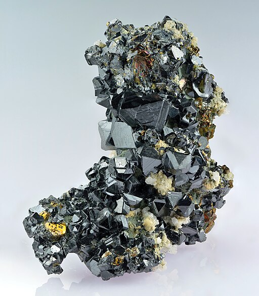
Unlike many industrial metals, minerals containing lead, silver, and zinc generally aren’t oxides of the metals. Rather, these three metals are far more likely to combine with sulfur, so their ores are mostly sulfide minerals. For lead, the primary ore is galena or lead (II) sulfide (PbS). Galena is a naturally occurring semiconductor, crystals of which lent their name to the early “crystal radios” which used a lump of galena probed with a fine cat’s whisker as a rectifier or detector for AM radio signals.

Geologically, galena is found in veins within various metamorphic rocks, and in association with a wide variety of sulfide minerals. Exactly what minerals those are depends greatly on the conditions under which the rock formed. Galena crystallized out of low-temperature geological processes is likely to be found in limestone deposits alongside other sulfide minerals such as sphalerite, or zincblende, an ore of zinc. When galena forms under higher temperatures, such as those associated with geothermal processes, it’s more likely to be associated with iron sulfides like pyrite, or Fool’s Gold. Hydrothermal galenas are also more likely to have silver dissolved into the mineral, classifying them as argentiferous ores. In some cases, such as the mines of the Silver Valley, the silver is at high enough concentrations that the lead is considered the byproduct rather than the primary product, despite galena not being a primary ore of silver.

Like a Lead Bubble

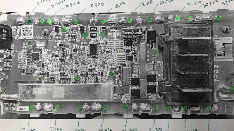
How galena is extracted and refined depends on where the deposits are found. In some places, galena deposits are close enough to the surface that open-cast mining techniques can be used. In the Silver Valley, though, and in other locations in North America with commercially significant galena deposits, galena deposits follow deep fissures left by geothermal processes, making deep tunnel mining more likely to be used. The scale of some of the mines in the Silver Valley is hard to grasp. The galena deposits that led to the Bunker Hill stake in the 1880s were found at an elevation of 3,600′ (1,100 meters) above sea level; the shafts and workings of the Bunker Hill Mine are now 1,600′ (488 meters) below sea level, requiring miners to take an elevator ride one mile straight down to get to work.

Ore veins are followed into the rock using a series of tunnels or stopes that branch out from vertical shafts. Stopes are cut with the time-honored combination of drilling and blasting, freeing up hundreds of tons of ore with each blasting operation. Loose ore is gathered with a slusher, a bucket attached to a dragline that pulls ore back up the stope, or using mining loaders, low-slung payloaders specialized for operation in tight spaces.

Ore plus soap equals metal bubbles. Froth flotation of copper sulfide is similar to the process for extracting zinc sulfide. Source: Geomartin, CC BY-SA 4.0

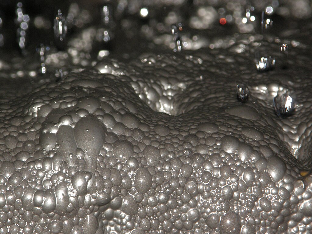
Silver Valley galena typically assays at about 10% lead, making it a fairly rich ore. It’s still not rich enough, though, and needs to be concentrated before smelting. Most mines do the initial concentration on site, starting with the usual crushing, classifying, washing, and grinding steps. Ball mills are used to reduce the ore to a fine powder, mixed with water and surfactants to form a slurry, and pumped into a broad, shallow tank. Air pumped into the bottom of the tanks creates bubbles in the slurry that carry the fine lead particles up to the surface while letting the waste rock particles, or gangue, sink to the bottom. It seems counterintuitive to separate lead by floating it, but froth flotation is quite common in metal refining; we’ve seen it used to concentrate everything from lightweight graphite to ultradense uranium. It’s also important to note that this is not yet elemental lead, but rather still the lead sulfide that made up the bulk of the galena ore.

Once the froth is skimmed off and dried, it’s about 80% pure lead sulfide and ready for smelting. The Bunker Hill Mine used to have the largest lead smelter in the world, but that closed in 1982 after decades of operation that left an environmental and public health catastrophe in its wake. Now, concentrate is mainly sent to smelters located overseas for final processing, which begins with roasting the lead sulfide in a blast of hot air. This converts the lead sulfide to lead oxide and gaseous sulfur dioxide as a waste product:

2 PbS + 3 O{_2} \rightarrow2 PbO + 2 SO{_2}

After roasting, the lead oxide undergoes a reduction reaction to free up the elemental lead by adding everything to a blast furnace fueled with coke:

2 PbO + C \rightarrow2 Pb + CO{_2}

Any remaining impurities float to the top of the batch while the molten lead is tapped off from the bottom of the furnace.

Zinc!

A significant amount of zinc is also located in the ore veins of the Silver Valey, enough to become a major contributor to the district’s riches. The mineral sphalerite is the main zinc ore found in this region; like galena, it’s a sulfide mineral, but it’s a mixture of zinc sulfide and iron sulfide instead of the more-or-less pure lead oxide in galena. Sphalerite also tends to be relatively rich in industrially important contaminants like cadmium, gallium, germanium, and indium.

Most sphalerite ore isn’t this pretty. Source: Ivar Leidus, CC BY-SA 4.0.

Extraction of sphalerite occurs alongside galena extraction and uses mostly the same mining processes. Concentration also uses the froth flotation method used to isolate lead sulfide, albeit with different surfactants specific for zinc sulfide. Concentration yields a material with about 50% zinc by weight, with iron, sulfur, silicates, and trace metals making up the rest.

Purification of zinc from the concentrate is via a roasting process similar to that used for lead, and results in zinc oxide and more sulfur dioxide:

2 ZnS + 3 O{_2}\rightarrow2 ZnO + 2SO{_2}

Originally, the Bunker Hill smelter just vented the sulfur dioxide out into the atmosphere, resulting in massive environmental damage in the Silver Valley. My neighbor relates his arrival in Idaho in 1970, crossing over the Lookout Pass from Montana on the then brand-new Interstate 90. Descending into the Silver Valley was like “a scene from Dante’s Inferno,” with thick smoke billowing from the smelter’s towering smokestacks trapped in the valley by a persistent inversion. The pine trees on the hillsides had all been stripped of needles by the sulfuric acid created when the sulfur dioxide mixed with moisture in the stale air. Eventually, the company realized that sulfur was too valuable to waste and started capturing it, and even built a fertilizer plant to put it to use. But the damage was done, and it took decades for the area to bounce back.

Recovering metallic zinc from zinc oxide is performed by reduction, again in a coke-fired blast furnace which collects the zinc vapors and condenses them to the liquid phase, which is tapped off into molds to create ingots. An alternative is electrowinning, where zinc oxide is converted to zinc sulfate using sulfuric acid, often made from the sulfur recovered from roasting. The zinc sulfate solution is then electrolyzed, and metallic zinc is recovered from the cathodes, melted, further purified if necessary, and cast into ingots.

Silver from Lead

If the original ore was argentiferous, as most of the Silver Valley’s galena is, now’s the time to recover the silver through the Parke’s process, a solvent extraction technique. In this case, the solvent is the molten lead, in which silver is quite soluble. The dissolved silver is precipitated by adding molten zinc, which has the useful property of reacting with silver while being immiscible with lead. Zinc also has a higher melting point than lead, meaning that as the temperature of the mixture drops, the zinc solidifies, carrying along any silver it combined with while in the molten state. The zinc-silver particles float to the top of the desilvered lead where they can be skimmed off. The zinc, which has a lower boiling point than silver, is driven off by vaporization, leaving behind relatively pure silver.

To further purify the recovered silver, cupellation is often employed. Cupellation is a pyrometallurgical process used since antiquity to purify noble metals by exploiting the different melting points and chemical properties of metals. In this case, silver contaminated with zinc is heated to the point where the zinc oxidizes in a shallow, porous vessel called a cupel. Cupels were traditionally made from bone ash or other materials rich in calcium carbonate, which gradually absorbs the zinc oxide, leaving behind a button of purified silver. Cupellation can also be used to purify silver directly from argentiferous galena ore, by differentially absorbing lead oxide from the molten solution, with the obvious disadvantage of wasting the lead:

Ag + 2 Pb + O{_2}\rightarrow 2PbO + Ag

Cupellation can also be used to recover small amounts of silver directly from refined lead, such as that in wheel weights:

If my grandfather had only known.

ROG Ally Community Rebuilds The Proprietary Asus eGPU

As far as impressive hacks go, this one is more than enough for your daily quota. You might remember the ROG Ally, a Steam Deck-like x86 gaming console that’s graced our pages a couple lf times. Now, this is a big one – from the ROG Ally community, we get a fully open-source eGPU adapter for the ROG Ally, built by reverse-engineering the proprietary and overpriced eGPU sold by Asus.

We’ve seen this journey unfold over a year’s time, and the result is glorious – two different PCBs, one of them an upgraded drop-in replacement board for the original eGPU, and another designed to fit a common eGPU form-factor adapter. The connector on the ROG Ally is semi-proprietary, but its cable could be obtained as a repair part. From there, it was a matter of scrupulous pinout reverse-engineering, logic analyzer protocol captures, ACPI and BIOS decompiling, multiple PCB revisions and months of work – what we got is a masterpiece of community effort.

Do you want to learn how the reverse-engineering process has unfolded? Check out the Diary.md – it’s certainly got something for you to learn, especially if you plan to walk a similar path; then, make sure to read up all the other resources on the GitHub, too! This achievement follows a trend from the ROG Ally community, with us having featured dual-screen mods and battery replacements before – if it continues the same way, who knows, maybe next time we will see a BGA replacement or laser fault injection.

Java Ring: One Wearable to Rule All Authentications

Today, you likely often authenticate or pay for things with a tap, either using a chip in your card, or with your phone, or maybe even with your watch or a Yubikey. Now, imagine doing all these things way back in 1998 with a single wearable device that you could shower or swim with. Sound crazy?

These types of transactions and authentications were more than possible then. In fact, the Java ring and its iButton brethren were poised to take over all kinds of informational handshakes, from unlocking doors and computers to paying for things, sharing medical records, making coffee according to preference, and much more. So, what happened?

Just Press the Blue Dot

Perhaps the most late-nineties piece of tech jewelry ever produced, the Java Ring is a wearable computer. It contains a tiny microprocessor with a million transistors that has a built-in Java Virtual Machine (JVM), non-volatile storage, and an serial interface for data transfer.

A family of Java iButton devices, including the Java Ring, a Java dog tag, and two Blue Dot readers -- one parallel, one serial.
A family of Java iButton devices and smart cards, including the Java Ring, a Java dog tag, and two Blue Dot readers. Image by [youbitbrain] via reddit
Technically speaking, this thing has 6 Kb of NVRAM expandable to 128 Kb, and up to 64 Kb of ROM (PDF). It runs the Java Card 2.0 standard, which is discussed in the article linked above.

While it might be the coolest piece in the catalog, the Java ring was just one of many ways to get your iButton. But wait, what is this iButton I keep talking about?

In 1989, Dallas Semiconductor created a storage device that resembles a coin cell battery and uses the 1-Wire communication protocol. The top of the iButton is the positive contact, and the casing acts as ground. These things are still around, and have many applications from holding bus fare in Istanbul to the immunization records of Canadian cows.

For $15 in 1998 money, you could get a Blue Dot receptor to go with it for sexy hardware two-factor authentication into your computer via serial or parallel port. Using an iButton was as easy as pressing the ring (or what have you) up against the Blue Dot.

Indestructible Inside and Out, Except for When You Need It

The mighty Java Ring on my left ring finger.
It’s a hefty secret decoder ring, that’s for sure.

Made of of stainless steel and waterproof grommets, this thing is built to be indestructible. The batteries were rated for a ten-year life, and the ring itself for one million hot contacts with Blue Dot receptors.

This thing has several types of encryption going for it, including 1024-bit RSA public-key encryption, which acts like a PGP key. There’s a random number generator and a real-time clock to disallow backdating transactions. And the processor is driven by an unstabilized ring oscillator, so it constantly varies its clock speed between 10 and 20 MHz. This way, the speed can’t be detected externally.

But probably the coolest part is that the embedded RAM is tamper-proof. If tampered with, the RAM undergoes a process called rapid zeroization that erases everything. Of course, while Java Rings and other iButton devices maybe be internally and externally tamper-proof, they can be lost or stolen quite easily. This is part of why the iButton came in many form factors, from key chains and necklaces to rings and watch add-ons. You can see some in the brochure below that came with the ring:

The front side of the Java Ring brochure, distributed with the rings.

The Part You’ve Been Waiting For

I seriously doubt I can get into this thing without totally destroying it, so these exploded views will have to do. Note the ESD suppressor.

An exploded view of the Java Ring showing the component parts. The construction of the iButton.

So, What Happened?

I surmise that the demise of the Java Ring and other iButton devices has to do with barriers to entry for businesses — even though receptors may have been $15 each, it simply cost too much to adopt the technology. And although it was stylish to Java all the things at the time, well, you can see how that turned out.

If you want a Java Ring, they’re on ebay. If you want a modern version of the Java Ring, just dissolve a credit card and put the goodies in resin.

iPhone 15 Gets Dual SIM Through FPC Patch

It can often feel like modern devices are less hackable than their thicker and far less integrated predecessors, but perhaps it’s just that our techniques need to catch up. Here’s an outstanding hack that adds a dual SIM slot to a US-sold eSIM iPhone 15/15 Pro, while preserving its exclusive mmwave module. No doubt, making use of the boardview files and schematics, it shows us that smartphone modding isn’t dead — it could be that we need to acknowledge the new tools we now have at our disposal.

When different hardware features are region-locked, sometimes you want to get the best of both worlds. This mod lets you go the entire length seamlessly, no bodges. It uses a lovely looking flexible printed circuit (FPC) patch board to tap into a debug header with SIM slot signals, and provides a customized Li-ion pouch cell with a cutout for the SIM slot. There’s just the small matter of using a CNC mill to make a cutout in the case where the SIM slot will go, and you’ll need to cut a buried trace to disable the eSIM module. Hey, we mentioned our skills needed to catch up, right? From there, it appears that iOS recognizes the new two SIM slots seamlessly.

The video is impressive and absolutely worth a watch if modding is your passion, and if you have a suitable CNC and a soldering iron, you can likely install this mod for yourself. Of course, you lose some things, like waterproofing, the eSIM feature, and your warranty. However, nothing could detract from this being a fully functional modkit for a modern-day phone, an inspiration for us all. Now, perhaps one of us can take a look at building a mod helping us do parts transplants between phones, parts pairing be damned.

Man-in-the-Middle PCB Unlocks HP Ink Cartridges

It’s a well-known secret that inkjet ink is being kept at artificially high prices, which is why many opt to forego ‘genuine’ manufacturer cartridges and get third-party ones instead. Many of these third-party ones are so-called re-manufactured ones, where a third-party refills an empty OEM cartridge. This is increasingly being done due to digital rights management (DRM) reasons, with tracking chips added to each cartridge. These chip prohibit e.g. the manual refilling of empty cartridges with a syringe, but with the right tweak or attack can be bypassed, with [Jay Summet] showing off an interesting HP cartridge DRM bypass using a physical man-in-the-middle-attack.

This bypass takes the form of a flex PCB with contacts on both sides which align with those on the cartridge and those of the printer. What looks like a single IC in a QFN package is located on the cartridge side, with space for it created inside an apparently milled indentation in the cartridge’s plastic. This allows is to fit flush between the cartridge and HP inkjet printer, intercepting traffic and presumably telling the printer some sweet lies so that you can go on with that print job rather than dash out to the store to get some more overpriced Genuine HP-approved cartridges.

Not that HP isn’t aware or not ticked off about this, mind. Recently they threatened to brick HP printers that use third-party cartridges if detected, amidst vague handwaving about ‘hackers’ and ‘viruses’ and ‘protecting the users’ with their Dynamic Security DRM system. As the many lawsuits regarding this DRM system trickle their way through the legal system, it might be worth it to keep a monochrome laser printer standing by just in case the (HP) inkjet throws another vague error when all you want is to just print a text document.

iZotope Ozone

Ozone by iZotope is a powerful audio mastering suite designed to help producers and sound engineers achieve professional-quality sound. This industry-standard tool offers a full set of modules for shaping and enhancing your tracks, including the new Clarity module for maximizing spectral power, Stem Focus for precise stem control, and Transient/Sustain for creative sound design. […]

Source

Fukushima Daiichi: Cleaning Up After a Nuclear Accident

On 11 March, 2011, a massive magnitude 9.1 earthquake shook the west coast of Japan, with the epicenter located at a shallow depth of 32 km,  a mere 72 km off the coast of Oshika Peninsula, of the Touhoku region. Following this earthquake, an equally massive tsunami made its way towards Japan’s eastern shores, flooding many kilometers inland. Over 20,000 people were killed by the tsunami and earthquake, thousands of whom were dragged into the ocean when the tsunami retreated. This Touhoku earthquake was the most devastating in Japan’s history, both in human and economic cost, but also in the effect it had on one of Japan’s nuclear power plants: the six-unit Fukushima Daiichi plant.

In the subsequent Investigation Commission report by the Japanese Diet, a lack of safety culture at the plant’s owner (TEPCO) was noted, along with significant corruption and poor emergency preparation, all of which resulted in the preventable meltdown of three of the plant’s reactors and a botched evacuation. Although afterwards TEPCO was nationalized, and a new nuclear regulatory body established, this still left Japan with the daunting task of cleaning up the damaged Fukushima Daiichi nuclear plant.

Removal of the damaged fuel rods is the biggest priority, as this will take care of the main radiation hazard. This year TEPCO has begun work on removing the damaged fuel inside the cores, the outcome of which will set the pace for the rest of the clean-up.

Safety Cheese Holes

Overview of a GE BWR as at Fukushima Daiichi. (Credit: WNA)
Overview of a GE reactor as at Fukushima Daiichi. (Credit: WNA)

The Fukushima Daiichi nuclear power plant was built between 1967 and 1979, with the first unit coming online in 1970 and the third unit by 1975. It features three generations of General Electric-designed boiling water reactors of a 1960s (Generation II) design. It features what is known as a Mark I containment structure. At the time of the earthquake only units 1, 2 and 3 were active, with the quake triggering safeties which shut down these reactors as designed. The quake itself did not cause significant damage to the reactors, but three TEPCO employees at the Fukushima Daiichi and Daini plants died as a result of the earthquake.

A mere 41 minutes later the first tsunami hit, followed by a second tsunami 8 minutes later, leading to the events of the Fukushima Daiichi accident. The too low seawall did not contain the tsunami, allowing water to submerge the land behind it. This damaged the seawater pumps for the main and auxiliary condenser circuits, while also flooding the turbine hall basements containing the emergency diesel generators and electrical switching gear. The backup batteries for units 1 and 2 also got taken out in the flooding, disabling instrumentation, control and lighting.

One hour after the emergency shutdown of units 1 through 3, they were still producing about 1.5% of their nominal thermal power. With no way to shed the heat externally, the hot steam, and eventually hydrogen from hot steam interacting with the zirconium-alloy fuel rod cladding, was diverted into the dry primary containment and then the wetwell, with the Emergency Core Cooling System (ECCS) injecting replacement water. This kept the cores mostly intact over the course of three days, with seawater eventually injected externally, though the fuel rods would eventually melt due to dropping core water levels, before solidifying inside the reactor pressure vessel (RPV) as well as on the concrete below it.

It was attempted to vent the steam pressure in unit 1, but this resulted in the hydrogen-rich air to flow into the service floor, where it found an ignition source and blew off the roof. To prevent this with unit 2, a blow-out panel was opened, but unit 3 suffered a similar hydrogen explosion on the service floor, with part of the hydrogen also making it into the defueled unit 4 via ducts and similarly blowing off its roof.

The hydrogen issue was later resolved by injecting nitrogen into the RPVs of units 1 through 3, along with external cooling and power being supplied to the reactors. This stabilized the three crippled reactors to the point where clean-up could be considered after the decay of the short-lived isotopes present in the released air. These isotopes consisted of mostly iodine-131, with a half-life of 8 days, but also cesium-137, with a half-life of 30 years, and a number of other isotopes.

Nuclear Pick-up Sticks

Before the hydrogen explosions ripped out the service floors and the building roofs, the clean-up would probably have been significantly easier. Now it seemed that the first tasks would consist out of service floor clean-up of tangled metal and creating temporary roofs to keep the elements out and any radioactive particles inside. These roof covers are fitted with cameras as well as radiation and hydrogen sensors. They also provide the means for a crane to remove fuel rods from the spent fuel pools at the top of the reactors, as most of the original cranes were destroyed in the hydrogen explosions.

Phot of the damaged unit 1 of Fukushima Daiichi and a schematic overview of the status. (Credit: TEPCO)

This meant that the next task is to remove all spent fuel from these spent fuel pools, with the status being tracked on the TEPCO status page. As units 5 and 6 were undamaged, they are not part of these clean-up efforts and will be retained after clean-up and decommissioning of units 1-4 for training purposes.

Meanwhile, spent fuel rods were removed already from units 3 and 4. For unit 1, a cover still has to be constructed as has has been done for unit 3, while for the more intact unit 2 a fuel handling facility is being constructed on the side of the building. Currently a lot of the hang-up with unit 1 is the removal of debris on the service floor, without risking disturbing the debris too much, like a gigantic game of pick-up sticks. Within a few years, these last spent fuel rods can then be safely transported off-site for storage, reprocessing and the manufacturing of fresh reactor fuel. That’s projected to be 2026 for Unit 2 and 2028 for Unit 1.

This spent fuel removal stage will be followed by removing the remnants of the fuel rods from inside the RPVs, which is the trickiest part as the normal way to defuel these three boiling-water reactors was rendered impossible due to the hydrogen explosions and the melting of fuel rods into puddles of corium mostly outside of the RPVs. The mostly intact unit number 2 is the first target of this stage of the clean-up.

Estimated corium distribution in Fukushima Daiichi unit 1 through 3. (Credit: TEPCO)

To develop an appropriate approach, TEPCO relies heavily on exploration using robotic systems. These can explore the insides of the units, even in areas which are deemed unsafe for humans and can be made to fit into narrow tubes and vents to explore even the insides of the RPVs. This is how we have some idea of where the corium ended up, allowing for a plan to be formed for the extracting of this corium for disposal.

Detailed updates on the progress of the clean-up can be found as monthly reports, which also provide updates on any changes noted inside the damaged units. Currently the cores are completely stable, but there is the ongoing issue of ground- and rainwater making it into the buildings, which causes radioactive particles to be carried along into the soil. This is why groundwater at the site has been for years now been pumped up and treated with the ALPS radioactive isotope removal system. This leaves just water with some tritium, which after mixing with seawater is released into the ocean. The effective tritium release this way is lower than when the Fukushima Daiichi plant was operating.

TEPCO employees connect pipes that push the 'Telesco' robot into the containment of Unit 2 for core sample retrieval. (Credit: TEPCO)
TEPCO employees connect pipes that push the ‘Telesco’ robot into the containment of Unit 2 for core sample retrieval. (Credit: TEPCO)

In these reports we also get updates on the robotic exploration, but the most recent update here involves a telescoping robot nicknamed ‘Telesco’ (because it can extend by 22 meters) which is tasked with retrieving a corium sample of a few grams from the unit 2 reactor, in the area underneath the RPV where significant amounts of corium have collected. This can then be analyzed and any findings factored into the next steps, which would involve removing the tons of corium. This debris consists of the ceramic uranium fuel, the zirconium-alloy cladding, the RPV steel and the transuranics and minor actinides like plutonium, Cs-137 and Sr-90, making it radiologically quite ‘hot’.

Looking Ahead

Although the clean-up of Fukushima Daiichi may seem slow, with a projected completion date decades from now, the fact of the matter is that time is in our favor, as the issue of radiological contamination lessens with every passing day. Although the groundwater contamination is probably the issue that gets the most attention, courtesy of the highly visible storage tanks, this is now fully contained including with sea walls, and there is even an argument to be made that dilution of radioisotopes into the ocean would make it a non-issue.

Regardless of the current debate about radiological overreacting and safe background levels, most of the exclusion zone around the Fukushima Daiichi plant has already been reopened, with only some zones still marked as ‘problematic’, despite having background radiation levels that are no higher than the natural levels in other inhabited regions of the world. This is also the finding of the UNSCEAR in their 2020 status report (PDF), which finds levels of Cs-137 in marine foods having dropped already sharply by 2015, no radiation-related events in those evacuated or workers in the exclusion zone, and no observed effects on the local fauna and flora.

Along with the rather extreme top soil remediation measures that continue in the exclusion zone, it seems likely that within a few years this exclusion zone will be mostly lifted, and the stricken plant itself devoid of spent fuel rods, even as the gradual removal of the corium will have begun. First starting with small samples, then larger pieces, until all that will left inside units 1-3 will be some radioactive dust, clearing the way to demolish the buildings. But it’s a long road.


Laser Fault Injection, Now With Optional Decapping

Whether the goal is reverse engineering, black hat exploitation, or just simple curiosity, getting inside the packages that protect integrated circuits has long been the Holy Grail of hacking. It isn’t easy, though; those inscrutable black epoxy blobs don’t give up their secrets easily, with most decapping methods being some combination of toxic and dangerous. Isn’t there something better than acid baths and spinning bits of tungsten carbide?

[Janne] over at Fraktal thinks so, and the answer he came up with is laser decapping. Specifically, this is an extension of the laser fault injection setup we recently covered, which uses a galvanometer-scanned IR laser to induce glitches in decapped microcontrollers to get past whatever security may be baked into the silicon. The current article continues that work and begins with a long and thorough review of various IC packaging technologies, including the important anatomical differences. There’s also a great review of the pros and cons of many decapping methods, covering everything from the chemical decomposition of epoxy resins to thermal methods. That’s followed by specific instructions on using the LFI rig to gradually ablate the epoxy and expose the die, which is then ready to reveal its secrets.

The benefit of leveraging the LFI rig for decapping is obvious — it’s an all-in-one tool for gaining access and executing fault injection. The usual caveats apply, of course, especially concerning safety; you’ll obviously want to avoid breathing the vaporized epoxy and remember that lasers and retinas don’t mix. But with due diligence, having a single low-cost tool to explore the innards of chips seems like a big win to us.

Reverse Engineering A Keyboard Driver Uncovers A Self-Destruct Code

Should you be able to brick a keyboard just by writing a driver to flash the lights on it? We don’t think so either. [TheNotary] got quite the shock when embarking on a seemingly straightforward project to learn C++ on the x86-64 architecture with Windows and sent it straight to Silicon Heaven with only a few seemingly innocent USB packets.

The project was a custom driver for the XVX S-K80 mechanical keyboard, aiming to flash LED patterns across the key LEDs and perhaps send custom images to the integrated LCD. When doing this sort of work, the first thing you need is the documentation of the communications protocols. Obviously, this was not an option with a closed-source project, so the next best thing is to spy on the existing Windows drivers and see how they worked. Using Wireshark to monitor the USB traffic whilst twiddling with the colour settings, it was clear that communications were purely over HID messages, simplifying subsequent analysis. Next, they used x32dbg (now x64dbg, but whatever) to attach to the existing driver process and trap a few interesting Windows system calls. After reading around the Windows API, a few candidate functions were identified and trapped. This gave them enough information to begin writing code to reproduce this behaviour. Then things got a bit odd.

There apparently was a lot of extra protocol baggage when performing simple tasks such as lighting an LED. They shortened the sequence to reduce the overhead and noticed an additional byte that they theorized must encode the number of packets to expect in case only a subset of the LEDs were being programmed. Setting this to 0x01 and sending LED code for single keys appeared to work and was much faster but seemed unreliable. After a short experiment with this mystery value, [TheNotary] reverted the code to send all the packets for the full LED set as before, forgetting to correct this mystery value from the 0xFF it was programmed to during the experiment. They were surprised that all the LEDs and LCD were switched off. They were then horrified when the keyboard never powered up again. This value appeared to have triggered an obscure firmware bug and bricked it—a sad end to what would have been a fun little learning project.

Keyboard hacks are so plentiful it’s hard to decide where to start. How about upgrading the keyboard of your trusty ZX81? Here’s a lovely, minimal mechanical keyboard powered by a Pi Pico, and finally while we’re thinking about drivers bricking your stuff, who can forget FTDI gate? We may never forgive that one.

Header image: Martin Vorel, CC BY-SA 4.0.

Maastr

Maastr is an AI-powered music mastering software that allows users to quickly and easily master their audio tracks. It features tools developed by sound engineers and also allows for collaborative feedback and revision tracking. It is suitable for both sound engineers and musicians looking to streamline their mastering process. With Maastr, users can upload their […]

Source

Train Speed Signaling Adapted For Car

One major flaw of designing societies around cars is the sheer amount of signage that drivers are expected to recognize, read, and react to. It’s a highly complex system that requires constant vigilance to a relatively boring task with high stakes, which is not something humans are particularly well adapted for. Modern GPS equipment can solve a few of these attention problems, with some able to at least show the current speed limit and perhaps an ongoing information feed of the current driving conditions., Trains, on the other hand, solved a lot of these problems long ago. [Philo] and [Tris], two train aficionados, were recently able to get an old speed indicator from a train and get it working in a similar way in their own car.

The speed indicator itself came from a train on the Red Line of the T, Boston’s subway system run by the Massachusetts Bay Transportation Authority (MBTA). Trains have a few unique ways of making sure they go the correct speed for whatever track they’re on as well as avoid colliding with other trains, and this speed indicator is part of that system. [Philo] and [Tris] found out through some reverse engineering that most of the parts were off-the-shelf components, and were able to repair a few things as well as eventually power everything up. With the help of an Arduino, an I/O expander, and some transistors to handle the 28V requirement for the speed indicator, the pair set off in their car to do some real-world testing.

This did take a few tries to get right, as there were some issues with the power supply as well as some bugs to work out in order to interface with the vehicle’s OBD-II port. They also tried to use GPS for approximating speed as well, and after a few runs around Boston they were successful in getting this speed indicator working as a speedometer for their car. It’s an impressive bit of reverse engineering as well as interfacing newer technology with old. For some other bits of train technology reproduced in the modern world you might also want to look at this recreation of a train whistle.

PC Floppy Copy Protection: Softguard Superlok

Many have sought the holy grail of making commercial media both readable and copy-proof, especially once everyone began to copy those floppies. One of these attempts to make floppies copy-proof was Softguard’s Superlok. This in-depth look at this copy protection system by [GloriousCow] comes on the heels of a part 1 that covers Formaster’s Copy-Lock. Interestingly, Sierra switched from Copy-Lock to Superlok for their DOS version of games like King’s Quest, following the industry’s quest in search of this holy grail.

The way that Superlok works is that it loads a (hidden) executable called CPC.COM which proceeds to read the 128 byte key that is stored on a special track 6. With this key the game’s executable is decoded and fun can commence. Without a valid ‘Play’ disk containing the special track and CPC.COM executable all one is instead left with is a request by the game to ‘insert your ORIGINAL disk 1’.

Sierra’s King Quest v1.0 for DOS.

As one can see in the Norton Commander screenshot of a Sierra game disk, the hidden file is easily uncovered in any application that supports showing hidden files. However, CPC.COM couldn’t be executed directly; it needs to be executed from a memory buffer and passed the correct stack parameters. Sierra likely put in very little effort when implementing Softguard’s solution in their products, as Superlok supports changing the encryption key offset and other ways to make life hard for crackers.

Sierra was using version 2.3 of Superlok, but Softguard would also make a version 3.0. This is quite similar to 2.x, but has a gotcha in that it reads across the track index for the outer sector. This requires track wrapping to be implemented. Far from this kind of copy protection cracking being a recent thing, there was a thriving market for products that would circumvent these protections, all the way up to Central Point’s Copy II PC Option Board that would man-in-the-middle between the floppy disk drive and the CPU, intercepting data and render those copy protections pointless.

As for the fate of Softguard, by the end of the 1980s many of its customers were tiring of the cat-and-mouse game between crackers and Softguard, along with issues reported by legitimate users. Customers like Infographics Inc. dropped the Superlok protection by 1987 and by 1992 Softguard was out of business.

Getting Root on Cheap WiFi Repeaters, the Long Way Around

What can you do with a cheap Linux machine with limited flash and only a single free GPIO line? Probably not much, but sometimes, just getting root to prove you can is the main goal of a project. If that happens to lead somewhere useful, well, that’s just icing on the cake.

Like many interesting stories, this one starts on AliExpress, where [Easton] spied some low-cost WiFi repeaters, the ones that plug directly into the wall and extend your wireless network another few meters or so. Unable to resist the siren song, a few of these dongles showed up in the mailbox, ripe for the hacking. Spoiler alert: although the attempt on the first device had some success by getting a console session through the UART port and resetting the root password, [Easton] ended up bricking the repeater while trying to install an OpenWRT image.

The second attempt, this time on a different but similar device, proved more fruitful. The rudimentary web UI provided no easy path in, although it did a pretty good job enumerating the hardware [Easton] was working with. With the UART route only likely to provide temptation to brick this one too, [Easton] turned to a security advisory about a vulnerability that allows remote code execution through a specially crafted SSID. That means getting root on these dongles is as simple as a curl command — no hardware hacks needed!

As for what to do with a bunch of little plug-in Linux boxes with WiFi, we’ll leave that up to your imagination. We like [Easton]’s idea of running something like Pi-Hole on them; maybe Home Assistant would be possible, but these are pretty resource-constrained machines. Still, the lessons learned here are valuable, and at this price point, let the games begin.

What’s New in 3D Scanning? All-In-One Scanning is Nice

3D scanning is important because the ability to digitize awkward or troublesome shapes from the real world can really hit the spot. One can reconstruct objects by drawing them up in CAD, but when there isn’t a right angle or a flat plane in sight, calipers and an eyeball just doesn’t cut it.

Scanning an object can create a digital copy, aid in reverse engineering, or help ensure a custom fit to something. The catch is making sure that scanning fits one’s needs, and isn’t more work than it’s worth.

I’ve previously written about what to expect from 3D scanning and how to work with it. Some things have changed and others have not, but 3D scanning’s possibilities remain only as good as the quality and ease of the scans themselves. Let’s see what’s new in this area.

All-in-One Handheld Scanning

MIRACO all-in-one 3D scanner by Revopoint uses a quad-camera IR structured light sensor to create 1:1 scale scans.

3D scanner manufacturer Revopoint offered to provide me with a test unit of a relatively new scanner, which I accepted since it offered a good way to see what has changed in this area.

The MIRACO is a self-contained handheld 3D scanner that, unlike most other hobby and prosumer options, has no need to be tethered to a computer. The computer is essentially embedded with the scanner as a single unit with a touchscreen. Scans can be previewed and processed right on the device.

Being completely un-tethered is useful in more ways than one. Most tethered scanners require bringing the object to the scanner, but a completely self-contained unit like the MIRACO makes it easier to bring the scanner to the subject. Scanning becomes more convenient and flexible, and because it processes scans on-board, one can review and adjust or re-scan right on the spot. This is more than just convenience. Taking good 3D scans is a skill, and rapid feedback makes practice and experimentation more accessible.

Features

The MIRACO resembles a chunky digital camera with an array of sensors at the front and a large touchscreen on the back. As a nice touch, the screen can be flipped out to let the scanner be used in “selfie” mode.

The structured light pattern as seen in IR, projected from the front of the device.

At its core, the MIRACO is a quad-camera IR structured light sensor. A pattern of infrared light is projected, and based on how this known pattern is observed by cameras to land on an object, the object’s topology can be inferred and eventually turned into a 3D model.

This method is sensitive to both exposure and focal distance, but the MIRACO tries to cover these bases by offering near and far focal modes (for small and large objects, respectively) as well as a live preview from which the user can judge scan conditions on the fly. Since the human eye cannot see IR, and most of us lack an intuitive sense of how IR interacts with different materials, this last feature is especially handy.

It’s worth mentioning that the models generated by the MIRACO’s scans are 1:1 with real-world dimensions. Having 3D models scaled to match the object they came from is stupendously useful when it comes to anything related to objects fitting into or around other objects.

Limitations

3D scanning is in general still not a foolproof, point-and-shoot process. As with photography, there is both a skill and an art to getting the best results. An operator has to do their part to give the sensor a good view of everything it needs.

Conditions Have to be Right

  • One needs to scan in an environment that is conducive to good results. Some materials and objects scan easier than others.
  • The scanner is particularly picky about focal length and exposure settings, and can be sensitive to IR interference and reflections. In terms of scanning with the MIRACO, this means the projected IR should be bright enough to illuminate the object fully while not being so bright that it washes out important features.
  • IR isn’t visible, so this isn’t easy to grasp intuitively. Happily, there’s a live display on the screen for both exposure and focus distance. This guides a user to stay within the sweet spots when scanning. Better results come easily with a bit of experience.

Scans Are Only as Good as the Weakest Link

  • The scanner only models what it can see. The holes in this 1-2-3 block for example are incomplete.

    There is a long chain of processes to go from raw sensor data to finished 3D model, and plenty of opportunity for scans to end up less than ideal along the way.

  • 3D scanners like to boast about scan quality with numbers like “0.02 mm accuracy”, but keep in mind that such numbers are best cases from the raw sensor itself.
  • When it comes right down to it, a generated model can only be as good as the underlying point cloud. The point cloud is only as good as the sensor data, and the quality of the sensor data is limited by the object and its environment.
  • Also, a scanner can only scan what it can see. If an internal void or channel isn’t visible from the scanner’s perspective, it won’t be captured in a scan.

It is not hard to get useful results with a little practice, but no one will be pointing a box and pressing a button to effortlessly receive perfect scans down to the last fraction of a millimeter anytime soon. Have realistic expectations about what is achievable.

Basic Workflow of a 3D Scan

Here is the basic process for scanning an object with the MIRACO that should give a good idea of what is involved.

Job Setup and Scan

A highly reflective object like a polished 1-2-3 block is best treated with a matte finish before scanning. Here I used AESUB Blue vanishing scanning spray, which evaporates in about an hour.

A scan begins by configuring the scanner via touchscreen with some basics like choosing Near or Far mode, object type, and whether to track features or markers. Because the scanner only sees a portion of the object at a time, the software stitches together many images from different angles to build the point cloud that is the foundation for everything else. Alignment of these partial scans is done on the fly either by tracking features (unique shapes on the object) or markers (reflective dots that can be applied as stickers, or printed on a mat.)

If an object is excessively glossy or reflective or otherwise difficult for the scanner to see properly, treat it with a surface coating for better results. One option is dusting it with talcum powder, another is a purpose-made 3D scanning spray like AESUB offers.

With object and scanner ready, The MIRACO is pointed like a camera and moved around the object (or the object spun on a turntable) while trying to stay an optimum distance away for best results. The screen gives feedback on this process, including a live display as the device stitches scans together.

Processing Results

Results can be viewed on the device, and generally speaking, if the scan quality is good then the automatic one-click model processing will easily generate a reasonable 3D model. If there’s a problem, one can continue scanning or try again.

Scans can be exported in a variety of formats via USB or over Wi-Fi. If Revopoint’s Revo Scan software is installed, additional editing and processing options are available such as merging multiple separate scans of an object or fine-tuning processing steps.

Using The Resulting Model

The resulting 3D model (a mesh output like .STL, .3MF, or .OBJ) may require additional processing or editing depending on what one wishes to do with it. A mesh editing program like Blender is full-featured, but Microsoft’s 3D Builder is pretty handy for many common tasks when it comes to editing and handling meshes. Most slicer software for 3D printers can handle basic things as well.

Example Scans and Projects

Here are a few scans and prints I did to illustrate the sort of results you should expect with a tool like this. Each of these highlights an important aspect of scanning from the context of part design and 3D printing. The MIRACO is also capable of scanning large objects, though I focus on smaller ones here.

Scanning a Part, Designing a Socket for that Part

This first example demonstrates scanning an object (in this case, a fan) in order to design a socket in another piece that will fit it perfectly.

To do this, I scanned the fan (including attached cable) then manually traced its vertical footprint in CAD. This created a sort of cutout object I could use to make a socket. Objects with more complex shapes can be cut into slices, and each sliced traced individually.

I’d like to point out that because the scan is being used as a reference for a CAD sketch, imperfect or otherwise incomplete scans can still be perfectly serviceable as long as the right parts of the object are intact.

Scanning a Hole and Printing a Plug

This is a great way to show the different possibilities and features in action, such as the fact that scans are 1:1 with their real-world subject.

I roughly chopped a hole out of a chunk of packing foam, scanned the hole, then 3D printed a model of the hole to use as a plug. It fits perfectly, and its shape even accurately captured small details I hadn’t noticed.

Custom Ergonomic Grip

3D scanning is a great way to capture objects with complex shapes that cannot be modeled by calipers and squinted eyeballs alone. Wearables and handhelds are one example, and here I demonstrate creating a custom, ergonomic grip.

I use modeling clay to create a custom hand grip, then scan the result. The scan is easily edited in terms of separating into halves, making a central hole for mounting, and 3D printing the result.

Note that I scanned this object in color (which the MIRACO is capable of) but the color scan serves no real function here other than being more visual.

Remaining Challenges

So what’s not new in 3D scanning? The tools and software are certainly better and easier to use, but some things remain challenging.

Some Objects Scan Better Than Others

Scanning is still fussy about how a subject is framed and shot, as well as how reflective it is or isn’t. Taking these into account is part of getting good results.

3D Scanners Output Meshes, Not CAD Models

I’ve explained before how meshes are fundamentally different from what one is usually working with in a CAD program when designing physical parts. “Widen this hole by 0.5 mm” or “increase this angle by 5 degrees” simply aren’t the kind of edits one easily does with a mesh.

Converting a Mesh to a CAD Format Remains Imperfect

Turning an .stl into an .stp (for example) still doesn’t have great options. Tools exist, but the good ones are mostly the domain of non-free CAD suites; the kind with hefty price tags on annual licenses.

The good news is that meshes not only 3D print just fine, they also work easily with basic Boolean operations (merge, subtract, scale) and can be used as references when modeling a part. Having a scan that is scaled 1:1 to real-world dimensions is a big help.

What’s Your Experience?

3D scanning is still a process that depends on and benefits greatly from a skilled operator, but it’s getting easier to use and easier to experiment with.

Photogrammetry is still an accessible way to do 3D scanning that requires no special hardware, but it lacks immediate feedback, and the resulting 3D model will not be a 1:1 match to real-world dimensions.

Have you found 3D scanning useful for something? What was the best part? The worst? We’d love to hear about it, so share your experience in the comments.

LinkedIn Goes All in on AI

LinkedIn recently announced several major new AI-powered products and features coming soon to the popular social media recruiting platform. The goal of these new tools is to streamline hiring and upskilling for HR professionals by utilizing artificial intelligence capabilities. In this article, we’ll go over a few of the key changes and upcoming AI features […]

Source

Reverse-Engineering the AMD Secure Processor Inside the CPU

On an x86 system the BIOS is the first part of the system to become active along with the basic CPU core(s) functionality, or so things used to be until Intel introduced its Management Engine (IME) and AMD its AMD Secure Processor (AMD-SP). These are low-level, trusted execution environments, which in the case of AMD-SP involves a Cortex-A5 ARM processor that together with the Cryptographic Co-Processor (CCP) block in the CPU perform basic initialization functions that would previously have been associated with the (UEFI) BIOS like DRAM initialization, but also loading of encrypted (AGESA) firmware from external SPI Flash ROM. Only once the AMD-SP environment has run through all the initialization steps will the x86 cores be allowed to start up.

In a detailed teardown by [Specter] over at the Dayzerosec blog the AMD-SP’s elements, the used memory map  and integration into the rest of the CPU die are detailed, with a follow-up article covering the workings of the CCP. The latter is used both by the AMD-SP as well as being part of the cryptography hardware acceleration ISA offered to the OS. Where security researchers are interested in the AMD-SP (and IME) is due to the fascinating attack vectors, with the IME having been the most targeted, but AMD-SP having its own vulnerabilities, including in related modules, such as an injection attack against AMD’s Secure Encrypted Virtualization (SEV).

Although both AMD and Intel are rather proud of how these bootstrapping systems enable TPM, secure virtualization and so on, their added complexity and presence invisible to the operating system clearly come with some serious trade-offs. With neither company willing to allow a security audit, it seems it’s up to security researchers to do so forcefully.

Unusual Tool Gets an Unusual Repair

In today’s value-engineered world, getting a decade of service out of a cordless tool is pretty impressive. By that point you’ve probably gotten your original investment back, and if the tool gives up the ghost, well, that’s what the e-waste bin is for. Not everyone likes to give up so easily, though, which results in clever repairs like the one that brought this cordless driver back to life.

The Black & Decker “Gyrodriver,” an interesting tool that is controlled with a twist of the wrist rather than the push of a button, worked well for [Petteri Aimonen] right up until the main planetary gear train started slipping thanks to stripped teeth on the plastic ring gear. Careful measurements of one of the planetary gears to determine parameters like the pitch and pressure angle of the teeth, along with the tooth count on both the planet gear and the stripped ring.

Here, most of us would have just 3D printed a replacement ring gear, but [Petteri] went a different way. He mentally rolled the ring gear out, envisioning it as a rack gear. To fabricate it, he simply ran a 60° V-bit across a sheet of steel plate, creating 56 parallel grooves with the correct pitch. Wrapping the grooved sheet around a round form created the ring gear while simultaneously closing the angle between teeth enough to match the measured 55° tooth angle in the original. [Petteri] says he soldered the two ends together to form the ring; it looks more like a weld in the photos, but whatever it was, the driver worked well after the old plastic teeth were milled out and the new ring gear was glued in place.

We think this is a really clever way to make gears, which seems like it would work well for both internal and external teeth. There are other ways to do it, of course, but this is one tip we’ll file away for a rainy day.

Ryobi Battery Pack Gives Up Its Secrets Before Giving Up the Ghost

Remember when dead batteries were something you’d just toss in the trash? Those days are long gone, thankfully, and rechargeable battery packs have put powerful cordless tools in the palms of our hands. But when those battery packs go bad, replacing them becomes an expensive proposition. And that’s a great excuse to pop a pack open and see what’s happening inside.

The battery pack in question found its way to [Don]’s bench by blinking some error codes and refusing to charge. Popping it open, he found a surprisingly packed PCB on top of the lithium cells, presumably the battery management system judging by the part numbers on some of the chips. There are a lot of test points along with some tempting headers, including one that gave up some serial data when the battery’s test button was pressed. The data isn’t encrypted, but it is somewhat cryptic, and didn’t give [Don] much help. Moving on to the test points, [Don] was able to measure the voltage of each battery in the series string. He also identified test pads that disable individual cells, at least judging by the serial output, which could be diagnostically interesting.  [Don]’s reverse engineering work is now focused on the charge controller chip, which he’s looking at through its I2C port. He seems to have done quite a bit of work capturing output and trying to square it with the chip’s datasheet, but he’s having trouble decoding it.

This would be a great place for the Hackaday community to pitch in so he can perhaps get this battery unbricked. We have to admit feeling a wee bit responsible for this, since [Don] reports that it was our article on reverse engineering a cheap security camera that inspired him to dig into this, so we’d love to get him some help.

RoEx Automix

RoEx Automix lets you mix and master your audio tracks using AI. Users can use Automix for free but the tool runs on a credit system, and you only get 1 credit per month as a free user. In my opinion the pricing is a little expensive for what they offer, however you can always […]

Source

❌