Vista de Lectura

Hay nuevos artículos disponibles. Pincha para refrescar la página.

Exploring TapTo NFC Integration On The MiSTer

[Ken] from the YouTube channel What’s Ken Making is back with another MiSTer video detailing the TapTo project and its integration into MiSTer. MiSTer, as some may recall, is a set of FPGA images and a supporting ecosystem for the Terasic DE10-Nano FPGA board, which hosts the very capable Altera Cyclone V FPGA.

The TeensyROM C64 cart supports TapTo

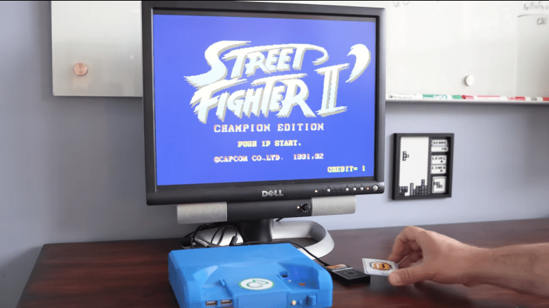
The concept behind TapTo is to use NFC cards, stickers, and other such objects to launch games and particular key sequences. This allows an NFC card to be programmed with the required FPGA core and game image. The TapTo service runs on the MiSTer, waiting for NFC events and launching the appropriate actions when it reads a card. [Ken] demonstrates many such usage scenarios, from launching games quickly and easily with a physical ‘game card’ to adding arcade credits and even activating cheat codes.

As [Ken] points out, this opens some exciting possibilities concerning physical interactivity and would be a real bonus for people less able-bodied to access these gaming systems. It was fun to see how the Nintendo Amiibo figures and some neat integration projects like the dummy floppy disk drive could be used.

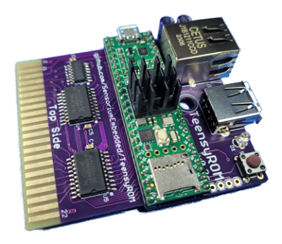
TapTo is a software project primarily for the MiSTer system, but ports are underway for Windows, the MiSTex, and there’s a working Commodore 64 game loader using the TeensyROM, which supports TapTo. For more information, check out the TapTo project GitHub page.

We’ve covered the MiSTer a few times before, but boy, do we have a lot of NFC hacks. Here’s an NFC ring and a DIY NFC tag, just for starters.

Thanks to [Stephen Walters] for the tip!

Archiving Data On Paper Using 2D Images

It seems like only yesterday we covered a project using QR codes to archive data on paper (OK, it was last Thursday), so here’s another way to do it, this time with a dedicated codec using the full page. Optar or OPTical ARchiver is a project capable of squeezing a whopping 200 Kb of data onto a single A4 sheet of paper, with writing and reading achieved with a standard laser printer and a scanner. It’s a bit harder than you might think to get that much data on the page, given that even a 600 DPI printer can’t reliably place every dot each time. Additionally, paper is rarely uniform at the microscopic scale, so Optar utilizes a forward error-correcting coding scheme to cater for a little irregularity in both printing and scanning.

The error-correcting scheme selected was an Extended Golay code (24, 12, 8),  which, interestingly, was also used for image transmission by the NASA Voyager 1 and 2 missions. In information theory terms, this scheme has a minimum Hamming Distance of 8, giving detection of up to seven bit errors. This Golay code implementation is capable of correcting three-bit errors in each 24-bit block, with 12 bits available for payload. That’s what the numbers in those brackets mean.

Another interesting problem is paper stretch during printing. A laser printer works by feeding the paper around rollers, some of which are heated. As a printer wears or gets dirty, the friction coefficient along the rollers can vary, leading to twisting and stretching of the paper during the printing process. Water absorbed by the paper can also lead to distortion. To compensate for these effects, Optar regularly inserts calibration targets throughout the bit image, which are used to locally resynchronize the decoding process as the image is processed. This is roughly similar to how the alignment patterns work within larger QR codes. Finally, similar to the position detection targets (those square bits) in QR codes, Optar uses a two-pixel-wide border around the bit image. The border is used to align to the corners well enough to locate the rows of bits to be decoded.

In the distant past of last week, we covered a similar project that uses QR codes. This got us thinking about how QR codes work, and even if encoding capacity can be increased using more colors than just black and white?

Thanks to [Petr] for the tip!

Taking Back The Internet With The Tildeverse

For many of us of a particular vintage, the internet blossomed in the ’90s with the invention of the Web and just a few years of development. Back then, we had the convenience of expression on the WWW and the backup of mature services such as IRC for all that other stuff we used to get up to. Some of us still hang out there. Then something happened. Something terrible. Big-commerce took over, and it ballooned into this enormously complex mess with people tracking you every few seconds and constantly trying to bombard you with marketing messages. Enough now. Many people have had enough and have come together to create the Tildeverse, a minimalist community-driven internet experience.

A collaborative Minecraft server hosted on a Tilde site

Tilde, literally ‘ ~ ‘, is your home on the internet. You can work on your ideas on a shared server or run your own. Tilde emphasises the retro aesthetic by being minimal and text-orientated. Those unfamiliar with a command line may start getting uncomfortable, but don’t worry—help is at hand. The number of activities is too many to list, but there are a few projects, such as a collaborative Sci-Fi story, a radio station, and even a private VoIP server. Gamers are catered for as long as you like Minecraft, but we think that’s how it should go.

The Tildeverse also supports Gopher and the new Gemini protocol,  giving some people a few more options with which to tinker. The usual method to gain access is to first sign up on a server, then SSH into it; you’re then taken to your little piece of the internet, ready to start your minimalist journey into the Tildeverse.

A couple of videos after the break go into much more detail about the whys and hows of the Tildeverse and are worth a chunk of your time.

We’ve talked about the ‘small web’ before. Here’s our guide to Gemini.

Thanks to [Andrew] for the tip!

Building A Multi-Purpose Electrochemistry Device

We don’t get enough electrochemistry hacks on these pages, so here’s [Markus Bindhammer] of YouTube/Marb’s lab fame to give us a fix with their hand-built general-purpose electrochemistry device.

The basic structure is made from plyboard cut to size on a table saw and glued’n’screwed together. The top and front are constructed from an aluminium sheet bent to shape with a hand-bender. A laser-printed front panel finishes the aesthetic nicely, contrasting with the shiny aluminium. The electrode holders are part of off-the-shelf chemistry components, with the electrical contacts hand-made from components usually used for constructing stair handrails. Inside, a 500 RPM 12 V DC geared motor is mounted, driving a couple of small magnets. A PWM motor speed controller provides power. This allows a magnetic stirrer to be added for relevant applications. Power for the electrochemical cell is courtesy of a Zk-5KX buck-boost power supply with a range of 0 – 36 V at up to 5 A  with both CV and CC modes. A third electrode holder is also provided as a reference electrode for voltammetry applications. A simple and effective build, we reckon!

Over the years, we’ve seen a few electrochemical hacks, like this DIY electroplating pen, a DIY electrochemical machining rig, and finally, a little something about 3D printing metal electrochemically.

Hacking an NVIDIA CMP 170HX Crypto GPU for EM Sim Work

A few years back NVIDIA created a dedicated cryptocurrency mining GPU, the CMP 170HX. This was a heavily restricted version of its flagship A100 datacenter accelerator, using the same GA100 chip. It was intended for accelerating Ethash, the Etherium proof-of-work algorithm, and nothing else. [niconiconi] bought one to use for accelerating PCB electromagnetic simulations and put a lot of effort into repairing the card, converting it to water-cooling, and figuring out how best to use this nobbled GPU.

Typically, the GA100 silicon sits in the center of the mighty A100 GPU card and would be found in a server rack, cooled by forced air. This was not an option at home, so an off-the-shelf water-cooling block was wedged in. During this process, [niconconi] found that the board wouldn’t power on, so they went on a deep dive into the power supply tree with the help of a leaked A100 schematic. The repair and modifications can be found in the appendix, right down to the end of the article. It is a long read to get there.

This Nvidia GA100 GPU is severely crippled on this board

NVIDIA has a history of deliberately restricting silicon in consumers’ hands to justify the hefty price tags of its offerings to big businesses, and this board is no different. The plan was to restrict the peak performance of the board to only applications with the same compute requirements as Ethash, specifically memory-intensive algorithms. The FP64 performance was severely limited, but instructions were not removed. This meant the code would run really badly, considering what the GPU is capable of.

The memory was limited to 8 GB, despite some A100 cards hosting a whopping 80 GB. The strategy was to use fuses to limit the crucial instructions, particularly the FP32 FMA and MAD instructions, which are used for multiply-add operations and are crucial for general computing applications. Finally, the PCIe bus was nobbled to run only as a Gen 1 interface with a single lane. They reduced the lane count by removing the coupling capacitors on the PCB, which meant they could just be added later, but it’s still only a slow interface.

[niconconi] went into great detail benchmarking the instruction types, keeping their EM simulation application in mind. After a few tweaks to make it work, they determined it was a good purchase. This article is worth reading for all those hardcore GPU nerds!

If you need a primer on GPU mining, we’ve got you covered. Once you’ve understood proof-of-work crypto, perhaps take a look at Chia?

Thanks to [gnif] for the tip!

Why have Seven Segments When You Can Have 21?

IO user [monte] was pointed towards an 1898 display patent issued to a [George Mason] and liked the look of the ‘creepy’ font it defined. The layout used no less than 21 discrete segments to display the complete roman alphabet and numerals, which is definitely not possible with the mere seven segments we are all familiar with. [monte] then did the decent thing and created a demonstration digit using modern parts.

For the implementation, [monte] created a simple PCB by hand (with an obvious mistake) and 3D-printed an enclosure and diffuser to match. After a little debugging, a better PCB was ordered from one of the usual overseas factories. There isn’t a schematic yet, but they mention using a CH32V003 Risc-V micro, which can be seen sitting on the rear of the PCB.

Maximum flexibility is ensured by storing every glyph as a 32-bit integer, with each LED corresponding to a single bit. It’s interesting to note the display incorporates serifs, which are definitely optional, although you could display sans-serif style glyphs if you wanted to. There is now a bit of a job to work out how to map character codes to glyph codes, but you can have a go at that yourself here. It’s still early doors on this project, but it has some real potential for a unique-looking display.

We love displays—every kind. Here’s a layout reminiscent of a VFD digit but done purely mechanically. And if you must limit yourself to seven digits, what about this unique thing?

DOOM on a Volumetric Display

There’s something magical about volumetric displays. They really need to be perceived in person, and no amount of static or video photography will ever do them justice. [AncientJames] has built a few, and we’re reporting on his progress, mostly because he got it to run a playable port of DOOM.

Base view of an earlier version showing the motor drive and PSU

As we’ve seen before, DOOM is very much a 3D game viewed on a 2D display using all manner of clever tricks and optimizations. The background visual gives a 3D effect, but the game’s sprites are definitely very solidly in 2D land. As we’ll see, that wasn’t good enough for [James].

The basic concept relies on a pair of 128 x 64 LED display matrix modules sitting atop a rotating platform. The 3D printed platform holds the displays vertically, with the LEDs lined up with the diameter, meaning the electronics hang off the back, creating some imbalance.

Lead, in the form of the type used for traditional window leading, was used as a counterbalance. A Raspberry Pi 4 with a modified version of this LED driver HAT is rotating with the displays. The Pi and both displays are fed power from individual Mini560 buck modules, taking their input from a 12 V 100 W Mean-Well power supply via a car alternator slip ring setup. (Part numbers ABH6004S and ASL9009  for those interested.) Finally, to synchronise the setup, a simple IR photo interrupter signals the Pi via an interrupt.

The second version running Doom

The base contains a DC motor driving the platform with a 224:20 reduction ratio using a GT2 timing belt to help reduce noise. [James] reports that running at 700 RPM was the limit for the current version, giving an acceptable update frame rate. Too high, and the vibration and chassis flex was excessive. The base does little else other than house that power supply and support a 400 mm acrylic garden light dome. We wouldn’t want to run this without such protection, which might not even be enough.

There are quite a few details to consider in such a build. One is the need to reduce the angle of perception of the LED display using a 3D printed slat-type collimator in front of each unit. You only want to perceive the LEDs head-on, or the POV effect is ruined. However, most of the details are in the software.

To that end, [James] took the entire game logic of the ‘Doom Generic’ port, removing the code that renders the 3D parts of the scene. The 2D menus and in-game panels are rendered by projecting the image onto a cylinder. That was easy. [James] took a minimalist path for the room scenes, as fully solid walls looked too busy. The viewport automatically zooms into any ongoing battles, so monsters zoom into focus if nearby, but objects behind closed doors and too far around corners are discarded. No spoiler alerts! The models were lifted from Chello’s Voxel Doom mod, giving a fitting 3D upgrade to gameplay. This is an ongoing project, so we’ll keep track and report back!

We’ve reported on a few volumetric displays over the years, like this tiny one based on an OLED display. Even a volumetric CCTV system. But they can’t run DOOM. Speaking of which, here’s what it looks like ray-traced.

Thanks to [Keith] for the tip!

Building a DIY MSX Mega Cartridge

[Mike] from Leaded Solder has a soft spot for old computers, and a chance encounter with a friend sent them deep down the deep hole that is the world of 80s and 90s-era Japanese home computers.  Many people playing with these machines have all kinds of issues to deal with, such as rotting cartridges, failing components, and just dirt and mank in critical places. [Mike] decided that working on an MSX-standard custom programmable cartridge would be sensible, but then got stuck on how the MSX cartridge mapping works.

The Konami 128K scheme uses 4 to 4-of-8 mapping.

You may recall that the MSX platform is not a single computer but a standard to which many (mainly Japanese) manufacturers designed their products. This disconnected the software writers from the hardware makers and is essentially a mirror of the IBM-PC clone scene.

The MSX is based around the Z80, which has a 16-bit address bus, restricting it to 64K of ROM or RAM. The MSX has two cartridge slots, an ‘internal’ slot for the BIOS and RAM and a fourth for ‘misc’ use. Each of these is mapped internally into the physical address space. The cartridge slots have 64K of addressable space mapped into the Z80 physical space.

If this was not complicated enough, many MSX games and applications exceeded this restriction and added a layer of mapping inside the cartridge using bank switching. A register in the cartridge could change the upper bits of the address allowing ROMs larger than 64K.

[Mike] wanted to replicate the method Konami used for their games. Their first target was The Maze of Galious, which requires a 128K ROM. Their scheme requires additional hardware to map each of the four 16K slots in the cartridge interface to four of the eight 16K slots of the ROM chip. The game selects which bits of the ROM it needs as the game progresses. The implementation uses an old 74LS670, which can still be bought from old stock as a 4×4 bit register file and a two-way dip selector switch. This allowed [Mike] to fit four games into a single SST39SF040 4MBit parallel flash chip. After a few false starts with the details of address bit selection, they were rewarded by Galious booting up without any additional work needed. If you own an MSX-compatible machine and want to build one for yourself, the full KiCAD project is available on the project GitHub page.

The MSX isn’t a well-known platform in the West, and MSX hacks are a rarity here, but in the spirit of retro, here’s a hack to add support for a retro gamepad to the MSX. Also, if you can’t find a period MSX, you can always build one.

Demonstrating The Photoelectric Effect Using Neon Lamps

Neon lamps are fun to play with. These old-school indicators were once heavily utilized in many types of equipment for indication purposes but now seem largely relegated to mains voltage indication duties. Here’s a fun video by [Ashish Derhgaen], discussing the photoelectric effect of neon lamps with some simple demonstrations.

Orange light makes it light!

[Ashish] demonstrates the well-known photoelectric effect by triggering a sub-biased neon lamp with visible light from an LED. Neon bulbs work on the principle of voltage-induced ionization, creating a visible glowing plasma. If the applied voltage is high enough, around 60 to 80 V, electrons get knocked off the neutral neon atoms. The now free electrons, roaming around highly energized, will eventually come across a neon ion (missing an electron) and recombine to make it neutral again.

The results are a lower total energy state, and the difference in energy is resolved by the emission of a photon of light, which, in the case of neon, is a dull reddish-orange. Nothing unusual there. However, nothing will happen if the applied voltage bias is just below this device-specific threshold. There’s not enough energy to strip electrons.

Apply an external light source, and this threshold can be exceeded. The photons from the LED are just energetic enough to strip a small number of electrons from the surface of the electrodes, and this causes a cascade, or avalanche effect, lighting up the plasma and turning on the neon lamp. Take away the external light source, and it dies down and goes dark.

The video also shows an interesting effect due to the wavelength of applied light. The photon energy needed to release an electron depends on the atom it strikes. Neon bulbs have all manner of electrode materials. [Ashish] shows that a particular neon lamp can be excited to emit a specific wavelength corresponding to a certain energy level. With some materials science work, this can then be used to ascertain what the electrode material is. Finally, the video shows some simple astable and relaxation oscillators initiated by light, making us wonder if one neon bulb could activate some neighboring bulbs and create a neat wave propagation effect for some electrode material and bias levels? You can see in the video that when the spectrum thrown from the prism is passed over the bulb, it illuminates in the orange section. So this could work. If you know, then do let us know with some examples.

Neon light hacks are plentiful around here. Neon lamps have many other uses beyond indication, even detecting sound. Of course, they look nice, but driving them is a hassle. Why not just fake the look with modern tech?

Exploring PC Floppy Protection: Formaster Copy-Lock

[GloriousCow] has started working on a series of investigations into the various historical floppy disk copy protection schemes used in the early days of the IBM PC and is here with the first of these results, specifically Formaster’s Copy-Lock.

This is the starting sector of track 6. It looks empty, but it’s not quite.

The game in question is King’s Quest by Sierra Entertainment, which used a ‘booter disk’ with the Copy-Lock protection scheme. Instead of having to boot DOS separately, you could just insert this disk and the game would launch automatically. Early copy protections often used simple methods, like adding sectors with non-standard sizes or tampering with sector CRC values to create disk errors. Copy-Lock employed several such tricks together, making it challenging for standard floppy disk hardware to replicate. In the case of Copy-Lock, Sector 1 on track 6 was intentionally written as only 256 bytes, with a 256-byte blank section to fill the gap. Additionally, the CRC was also altered to add another layer of protection.

When attempting to read the disk, the PC BIOS interrupt routine assumes it’s looking for a standard 512-byte sector, so when a “read sector” command is issued to locate the sector, it never finds it. To detect a dodgy copy, the game bypasses the BIOS and talks directly to the floppy disk controller using some custom code. The first part of the code uses the standard INT 13h routine to seek to track 6, sector 1, where it expects a fail since there is no valid sector there. Next, the floppy controller sends the “read track” command to perform a raw dump of all 512 bytes at this address and looks for a magic number, 0xF7, sitting in the final byte. That empty second half of the short sector is indeed not empty and is the check the game makes to determine if it was written with the Copy-Lock capable hardware. That last point is pertinent; you can’t create this disk structure with a standard IBM PC floppy disk controller; you need specialised hardware that can write different-sized sectors and incorrect CRCs, and that costs money to acquire.

We recently covered the copy protection scheme used for Dungeon Master on the Atari ST and the Amiga. If you’re thinking less about how a floppy got cracked and copied and more about how to preserve these digital relics, check this out!

Hardware Reuse: The PMG001 Integrated Power Management Module

Battery management is a tedious but necessary problem that becomes more of a hassle with lithium-ion technology. As we’re all very aware, such batteries need a bit of care to be utilized safely, and as such, a huge plethora of ICs are available to perform the relevant duties. Hackaday.IO user [Erik] clearly spent some time dropping down the same old set of ICs to manage a battery in their applications, so they created a drop-in castellated PCB to manage all this.

The little board, measuring just a smidge over 22 x 16mm, packs a fair amount of capability, with an ATTiny1616 to make it customisable. The Injoinic tech IP2312, which is intended to be supplied from USB sources, takes care of charging with a programmable current set by a resistor, as is typical. The battery output is switched by a beefy MOSFET, with the output first passing through a measurement resistor and being sensed by an INA219 bidirectional current monitor. This might be useful for monitoring charging via the microcontroller. An APX803 low-voltage lockout/supervisor IC enables an LD56100 LDO to ensure no load is supplied to the battery below the low-voltage threshold. This is important! This provides a 3.3V rail to all the other ICs on the board, which is always on when the battery voltage is high enough. Utilising interrupts in the ATTiny firmware means the controller remains mostly asleep, consuming as little power as possible and preserving battery standby time. Temperature measurement is courtesy of the TMP102 with a ADS1015 quad channel 12-bit delta-sigma ADC also wedged in for some auxiliary sensing. These additional analog channels are not actually used by the module but are presented on the IOs. These could be very handy for detecting external inputs relevant to battery management with some custom Arduino-compatible firmware.

Implementation-wise, [Erik] provides PCB footprint details for both Eagle and KiCAD and an example application circuit detailing hookup and programming. So long as you ensure the UDPI pin in connected to a UART as shown in the application circuit, developing and uploading custom application code should be simple. Check out the project GitHub for more details.

Topics of power management and batteries are plentiful. Here’s a nice, hackable power meter for starters. Here’s an interesting story about extracting perfectly useable LiPo cells from perfectly useless disposable vapes and, finally, a possible method for mitigating electrode damage due to constant current charging.

Fast 3D Printing With a Polar, Four Quadrant Custom Machine

3D printing is all well and good for making low numbers of units, so long as they’re small enough to print in a reasonable time, but what if you want to go really big? Does a 35-hour print time sound like a fun time? Would it even make it that long? [Nathan] from Nathan Build Robots didn’t fancy the wait, so they embarked on a project to build a huge parallel 3D printer with four independent print heads. Well, kind of.

Checkout this cool multi-material print with this weird shimmering effect

The premise seems obvious at first glance: More print heads mean more plastic is laid down per unit of time. As long as you can maximise the nozzle diameter and machine speed, it should theoretically be possible to speed things up massively. But it doesn’t work like that. The custom machine they constructed utilises a polar coordinate system, with a rotating bed (the ‘theta’ axis) and four radial axis gantries arranged at 90 degrees to each other. Each gantry has its own independent extruder, so multilateral printing is also an upfront option. [Nathan] laments that the problem with constructing such a beast is not so much the mechanical aspects but the limitations in the current firmwares out in the wild. There are also more complex considerations at the slicing level, so getting the machine to operate as desired is quite a large programming task! Right now, this means that each radial axis must operate in lock-step, meaning objects to be printed must be rotationally symmetric of order four. Another option is to print four copies of a much smaller object in parallel, which has its use cases, but that’s not their end goal. [Nathan] says he was going for a record-breaking 20kg print. However, multiple issues with alignment over height and bed adhesion, not to mention keeping the extruders fed with fresh filament, scuppered this first attempt.

There are some large hurdles regarding alignment. The four corner verticals can be out of alignment with each other in all sorts of ways, causing the radial axis to shift as the Z axis moves. We suspect that’s just one glaring problem, and other more subtle issues are waiting in the wings to cause problems in the future, but we’ll keep an eye on this and see where it goes!

We covered a few projects turning up the 3D printing knobs lately. Here’s a big printer, for big prints. Our thoughts about speed printing and, lastly, a fascinating machine mod that optimises colour swapping by having automated hot end swapping.

Using a 2D Scanner to Make 3D Things

[Chuck Hellebuyck] wanted to clone some model car raceway track and realised that by scanning the profile section of the track with a flatbed scanner and post-processing in Tinkercad, a useable cross-section model could be created. This was then extruded into 3D to make a pretty accurate-looking clone of the original part. Of course, using a flatbed paper scanner to create things other than images is nothing new, if you can remember to do it. A common example around here is scanning PCBs to capture mechanical details.

The goal was to construct a complex raceway for the grandkids, so he needed numerous pieces, some of which were curved and joined at different angles to allow the cars to race downhill. After printing a small test section using Ninjaflex, he found a way to join rigid track sections in curved areas. It was nice to see that modern 3D printers can handle printing tall, thin sections of this track vertically without making too much of a mess. This fun project demonstrates that you can easily combine 3D-printed custom parts with off-the-shelf items to achieve the desired result with minimal effort.

Flatbed scanner hacks are so plentiful it’s hard to choose a few! Here’s using a scanner to recreate a really sad-looking PCB, hacking a scanner to scan things way too big for it, and finally just using a scanner as a linear motion stage to create a UV exposure unit for DIY PCBs.

A Simple Guide to RF PCB Design

[Hans Rosenberg] knows a thing or two about RF PCB design and has provided a three-part video demonstration of some solid rules of thumb. We will cover the first part here, and leave the other two for the more interested readers!

The design process begins with a schematic diagram, assuming ideal conductors. Advanced software tools can extract the resistive, inductive, and capacitive elements of the physical wiring to create a parasitic model that can be compared to the desired schematic. The RF designer’s task is to optimize the layout to minimize differences and achieve the best performance to meet the design goals. However, what do you do when you don’t have access to such software?

[Hans] explains that at low frequencies, return current flows through all paths, with the lowest resistance path taking most of the current. At higher frequencies, the lowest inductance path carries all the current. In real designs, a ground plane is used instead of an explicit return trace for the lowest possible impedance.

You really wouldn’t design an RF circuit like this.

[Hans] shows the effect of interrupting the signal return path on a physical test PCB. The result is pretty bad, with the current forced to detour around the hole in the ground plane. A nanoVNA shows a -20 dB drop at 4 GHz, where the ground plane has effectively become an antenna. Energy will be radiated out, causing signal loss, but worse, it will create an EMC hazard with an unintended transmission.

Additionally, this creates an EMC susceptibility, making the situation worse. Placing a solder blob to bridge the gap directly under the signal trace is all that’s required to make it a continuous straight path again, and the performance is restored.

Floating planes are also an issue in RF designs, causing signal resonance and losses. One solution is to pull back the planes near the signal or stitch them to the ground plane with vias placed closely on either side of the signal trace. However, such stitching may slightly affect transmission line impedance and require tweaking the design a little. The next two parts of the series expand on this, hammering home the importance of good ground plane design. These are definitely worth a watch!

PCB design is as much art as science, and we’ve discussed this subject a lot. Here’s our simple guide to rocking RF PCB designs. There’s also a lot of devil in that detail, for example when understanding edge-launch SMA connectors.

An Open Source 6kW GaN Motor Controller

We don’t know how you feel when designing hardware, but we get uncomfortable at the extremes. High voltage or current, low noise figures, or extreme frequencies make us nervous.  [Orion Serup] from CrabLabs has been turning up a few of those variables and has created a fairly beefy 3-phase motor driver using GaN technology that can operate up to 80V at 70A. GaN semiconductors are a newer technology that enables greater power handling in smaller packages than seems possible, thanks to high electron mobility and thermal conductivity in the material compared to silicon.

The KiCAD schematic shows a typical high-power driver configuration, broken down into a gate pre-driver, the driver itself, and the following current and voltage sense sub-circuits. As is typical with high-power drivers, these operate in a half-bridge configuration with identical N-channel GaN transistors (specifically part EPC2361) driven by dedicated gate drivers (that’s the pre-driver bit) to feed enough current into the device to enable it to switch quickly and reliably.

The design uses the LM1025 low-side driver chip for this task, as you’d be hard-pushed to drive a GaN transistor with discrete components! You may be surprised that the half-bridge driver uses a pair of N-channel devices, not a symmetric P and N arrangement, as you might use to drive a low-power DC motor. This is simply because, at these power levels, P-channel devices are a rarity.

Why are P-channel devices rare? N-channel devices utilise electrons as the majority charge carrier, but P-channel devices utilise holes, and the mobility of holes in GaN is very low compared to that of electrons, resulting in much worse ON-resistance in a P-channel and, as a consequence, limited performance. That’s why you rarely see P-channel devices in a circuit like this.

Of course, schematic details are only part of the problem. High-power design at the PCB level also requires careful consideration. As seen from the project images, this involves heavy, thick copper traces on two or more heavily via-stitched layers to maximise copper volume and lower resistance as far as possible.  But, you can overdo this and end up with too much inductance in critical areas, quickly killing many high-power devices. Another vital area is the footprint design for the GaN device and how it connects to the rest of the circuit. Get this wrong or mess up the soldering, and you can quickly end up with a much worse performance!

We’ve seen DIY high-power controllers here a few times. Here’s an EV controller that uses discrete power modules. Another design we saw a few years ago drives IGBTs for a power output of 90kW.

❌