Vista de Lectura

Hay nuevos artículos disponibles. Pincha para refrescar la página.

Register Renaming: The Art of Parallel Processing

Close-up of a CPU

In the quest for faster computing, modern CPUs have turned to innovative techniques to optimize instruction execution. One such technique, register renaming, is a crucial component that helps us achieve the impressive multi-tasking abilities of modern processors. If you’re keen on hacking or tinkering with how CPUs manage tasks, this is one concept you’ll want to understand. Here’s a breakdown of how it works and you can watch the video, below.

In a nutshell, register renaming allows CPUs to bypass the restrictions imposed by a limited number of registers. Consider a scenario where two operations need to access the same register at once: without renaming, the CPU would be stuck, having to wait for one task to complete before starting another. Enter the renaming trick—registers are reassigned on the fly, so different tasks can use the same logical register but physically reside in different slots. This drastically reduces idle time and boosts parallel tasking. Of course, you also have to ensure that the register you are using has the correct contents at the time you are using it, but there are many ways to solve that problem. The basic technique dates back to some IBM System/360 computers and other high-performance mainframes.

Register renaming isn’t the only way to solve this problem. There’s a lot that goes into a superscalar CPU.
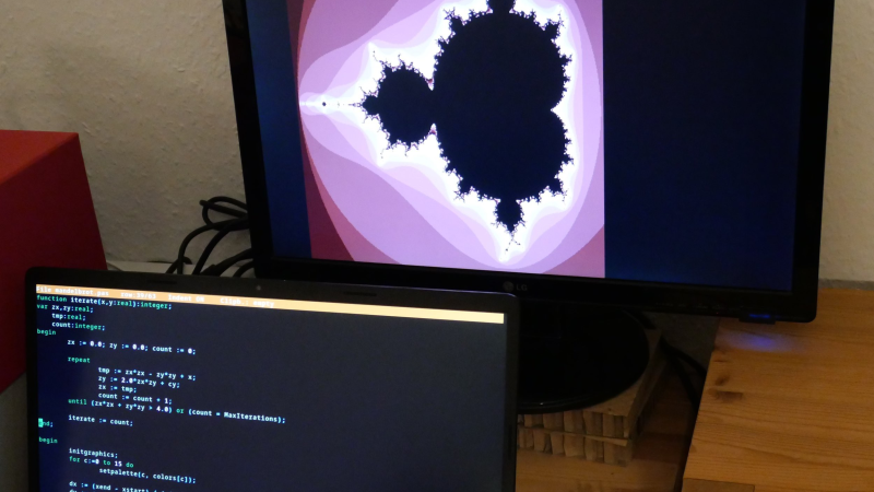
Tridora: A Full-Custom CPU Designed For Pascal

[Sebastian Lederer] has created Tridora: an unusual stack-based CPU core intended for FPGA deployment, co-developed with its own Pascal compiler. The 32-bit word machine is unusual in that it has not one but three stacks, 16-bit instruction words, and a limited ISA, more like those of the 8-bit world. No multiply or divide instructions will be found in this CPU.

The design consists of about 500 lines of Verilog targeting the Digilent Arty-A7 FPGA board, which is based around the Xilinx Artix-7 FPGA line. [Sebastian] plans to support the Nexys A7 board, which boasts a larger FPGA array but has less RAM onboard. The CPU clocks in at 83 MHz with four clock cycles per instruction, so over 20 MIPS, which is not so shabby for a homebrew design. Wrapped around that core are a few simple peripherals, such as the all-important UART, an SD card controller and a VGA display driver. On the software side, the Pascal implementation is created from scratch with quite a few restrictions, but it can compile itself, so that’s a milestone achieved. [Sebastian] also says there is a rudimentary operating system, but at the moment, it’s a little more than a loader that’s bundled with the program image.

The Tridora Gitlab project hosts the Verilog source, an emulator (written in Golang, not Pascal) and a suite of example applications. We see quite a few custom CPUs, often using older or less popular programming languages. Here’s an FPGA-based Forth machine to get you started. Implementing programming languages from scratch is also a surprisingly common hack. Check out this from-scratch compiler for the Pretty Laughable Programming language.

❌