Turning Down the Noise on SMPS
On paper, electricity behaves in easy-to-understand, predictable ways. That’s mostly because the wires on the page have zero resistance and the switching times are actually zero, whereas in real life neither of these things are true. That’s what makes things like switch-mode power supplies (SMPS) difficult to build and troubleshoot. Switching inductors and capacitors tens or hundreds of thousands of times a second (or more) causes some these difficulties to arise when these devices are built in the real world. [FesZ Electronis] takes a deep dive into some of the reasons these difficulties come up in this video.
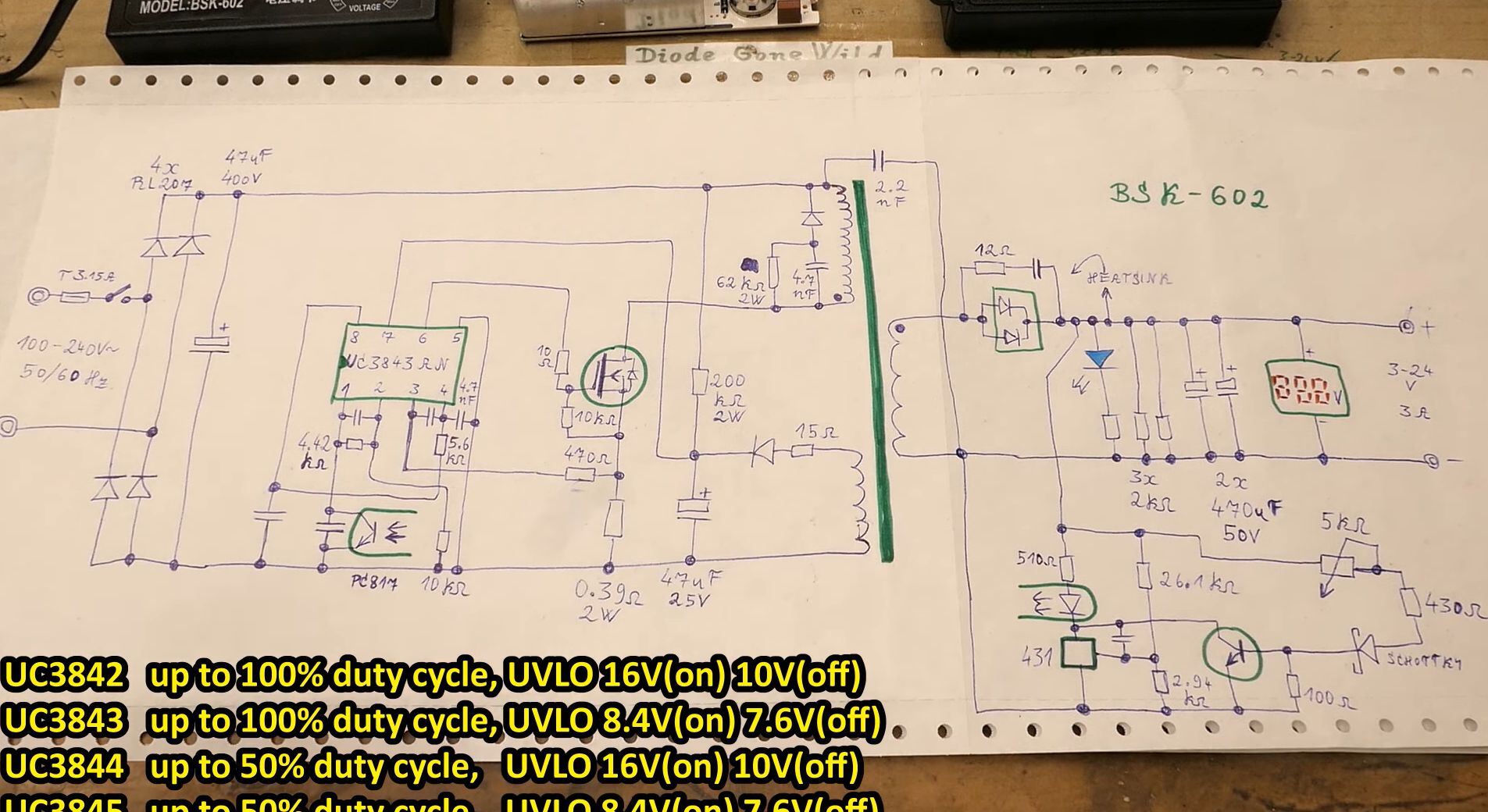
The first piece of electronics that can generate noise in an SMPS are the rectifier diodes. These have a certain amount of non-ideal capacitance as well as which causes a phenomenon called reverse current, but this can be managed by proper component choice to somewhat to limit noise.
The other major piece of silicon in power supplies like this that drives noise are the switching transistors. Since the noise is generally caused by the switching itself, there is a lot that can be done here to help limit it. One thing is to slow down the amount of time it takes to transition between states, limiting the transients that form as a result of making and breaking connections rapidly. The other, similar to selecting diodes, is to select transistors that have properties (specifically relating to inherent capacitances) that will limit noise generation in applications like this.
Of course there is a lot more information as well as charts and graphs in [FesZ]’s video. He’s become well-known for deep dives into practical electrical engineering topics like these for a while now. We especially like his videos about impedance matching as well as a more recent video where he models a photovoltaic solar panel in SPICE.