Don’t pack your bags for the trip to exoplanet K2-18b quite yet — it turns out that the James Webb Space Telescope may not have detected signs of life there after all. Last year, astronomers reported the possible presence of dimethyl sulfide there, a gas that (at least on Earth) is generally associated with phytoplankton in the ocean. Webb used its infrared spectrometer instruments to look at the light from the planet’s star, a red dwarf about 111 light-years away, as it passed through the hydrogen-rich atmosphere. The finding was sort of incidental to the discovery of much stronger signals for methane and carbon dioxide, but it turns out that the DMS signal might have just been overlap from the methane signal. It’s too bad, because K2-18b seems to be somewhat Earth-like, if you can get over the lack of oxygen and the average temperature just below freezing. So, maybe not a great place to visit, but it would be nice to see if life, uh, found a way anywhere else in the universe.
Attention Fortran fans: your favorite language isn’t quite dead yet. In fact, it cracked the top ten on one recent survey, perhaps on the strength of its numerical and scientific applications. The “Programming Community Index” is perhaps a bit subjective, since it’s based on things like Google searches for references to particular languages. It’s no surprise then that Python tops such a list, but it’s still interesting that there’s enough interest in a 67-year-old programming language to make it onto the list. We’d probably not advise building a career around Fortran, but you never know.
If your experience with Bluetooth is anything like ours, you’ll probably be skeptical of reports of a successful Bluetooth connection with a satellite 600 km in space. But according to Hubble Network, a startup seeking to build a global Bluetooth network, they managed to do it using off-the-shelf hardware. The feat apparently required a firmware update to account for the Doppler shift and a phased-array antenna on the satellite for beam steering, but other than that, direct Bluetooth connections from your phone to a satellite could be coming soon. For some reason.
If you’ve ever wondered why it costs $20 billion to build a semiconductor fab, wonder no more. This is a long article, but it has to be since it covers everything from the structure of semiconductor chips to the processes used to make them, and just about everything you ever wanted to know about fab construction. Our revelation was just how little of a fab’s vertical space is devoted to the cleanroom space, which is sandwiched between sub-fab and utility layers below and a huge interstitial space above for air handling. It’s eye-opening stuff.
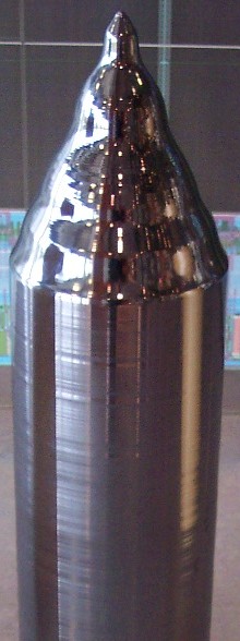
And finally, it turns out that “WarGames” was actually pretty accurate, at least in terms of the missile launch bunker set during the film’s cold open. Judging by this virtual tour of a US Minuteman ICBM launch control center (LCC), that is. The 360 tour features detailed — but not too detailed — photos of what appears to be an actual LCC and good explanations of all the equipment. Our biggest surprise was the pair of pink fuzzy bunny slippers in the commander’s kit bag. Hey, if you’re going to be responsible for potentially initiating the apocalypse, you might as well be comfortable.