The Flash Memory Lifespan Question: Why QLC May Be NAND Flash’s Swan Song
The late 1990s saw the widespread introduction of solid-state storage based around NAND Flash. Ranging from memory cards for portable devices to storage for desktops and laptops, the data storage future was prophesied to rid us of the shackles of magnetic storage that had held us down until then. As solid-state drives (SSDs) took off in the consumer market, there were those who confidently knew that before long everyone would be using SSDs and hard-disk drives (HDDs) would be relegated to the dust bin of history as the price per gigabyte and general performance of SSDs would just be too competitive.
Fast-forward a number of years, and we are now in a timeline where people are modifying SSDs to have less storage space, just so that their performance and lifespan are less terrible. The reason for this is that by now NAND Flash has hit a number of limits that prevent it from further scaling density-wise, mostly in terms of its feature size. Workarounds include stacking more layers on top of each other (3D NAND) and increasing the number of voltage levels – and thus bits – within an individual cell. Although this has boosted the storage capacity, the transition from single-level cell (SLC) to multi-level (MLC) and today’s TLC and QLC NAND Flash have come at severe penalties, mostly in the form of limited write cycles and much reduced transfer speeds.
So how did we get here, and is there life beyond QLC NAND Flash?
Floating Gates
At the core of NAND Flash lies the concept of floating gates, as first pioneered in the 1960s with the floating-gate MOSFET (FGMOS). As an FGMOS allows for the retention of a charge in the floating gate, it enabled the development of non-volatile semiconductor storage technologies like EPROM, EEPROM and flash memory. With EPROM each cell consists out of a single FET with the floating and control gates. By inducing hot carrier injection (HCI) with a programming voltage on the control gate, electrons are injected into the floating gate, which thus effectively turns the FET on. This allows then for the state of the transistor to be read out and interpreted as the stored bit value.
Naturally, just being able to program an EPROM once and then needing to erase the values by exposing the entire die to UV radiation (to induce ionization within the silicon oxide which discharges the FET) is a bit of a bother, even if it allowed the chip to be rewritten thousands of times. In order to make EPROMs in-circuit rewritable, EEPROMs change the basic FET-only structure with two additional transistors. Originally EEPROMs used the same HCI principle for erasing a cell, but later they would switch to using Fowler-Nordheim tunneling (FNT, the wave-mechanical form of field electron emission) for both erasing and writing a cell, which removes the damaging impact of hot carrier degradation (HCD). HCD and the application of FNT are both a major source of the physical damage that ultimately makes a cell ‘leaky’ and rendering it useless.
Combined with charge trap flash (CTF) that replaces the original polycrystalline silicon floating gate with a more durable and capable silicon nitride material, modern EEPROMs can support around a million read/write cycles before they wear out.
Flash memory is a further evolution of the EEPROM, with the main distinctions being a focus on speed and high storage density, as well as the use of HCI for writes in NOR Flash, due to the speed benefits this provides. The difference between NOR and NAND Flash comes from the way in which the cells are connected, with NOR Flash called that way because it resembles a NOR gate in its behavior:
To write a NOR Flash cell (set it to logical ‘0’), an elevated voltage is applied to the control gate, inducing HCI. To erase a cell (reset to logical ‘1’), a large voltage of opposite polarity is applied to the control gate and the source terminal, which draws electrons out of the floating gate due to FNT.
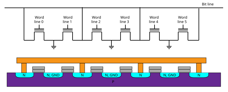
Reading a cell is then performed by pulling the target word line high. Since all of the storage FETs are connected to both ground and the bit line, this will pull the bit line low if the floating gate is active, creating a logical ‘1’ and vice versa. NOR Flash is set up to allow for bit-wise erasing and writing, although modern NOR Flash is moving to a model in which erasing is done in blocks, much like with NAND Flash:
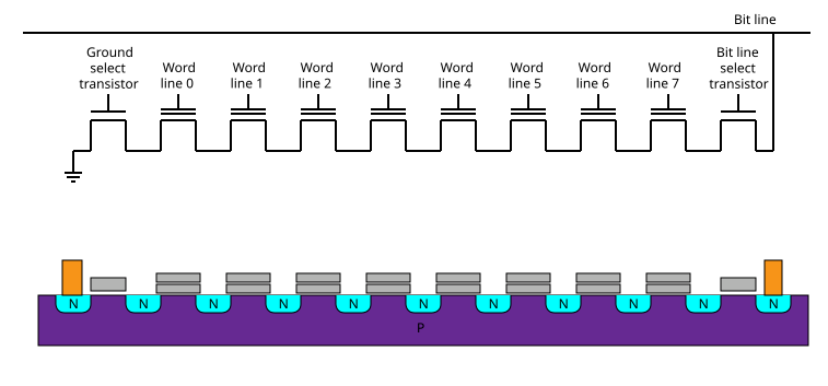
The reason why NAND Flash is called this way is readily apparent from the way the cells are connected, with a number of cells connected in series (a string) between the bit line and ground. NAND Flash uses FNT for both writing and erasing cells, which due to its layout always has to be written (set to ‘0’) and read in pages (a collection of strings), while erasing is performed on a block level (a collection of pages).
Unlike NOR Flash and (E)EPROM, the reading out of a value is significantly more complicated than toggling a control gate and checking the level of the bit line. Instead the control gate on a target cell has to be activated, while putting a much higher (>6V) voltage on the control gate of unwanted cells in a string (which turns them on no matter what). Depending on the charge inside the floating gate, the bit line voltage will reach a certain level, which can then be interpreted as a certain bit value. This is also how NAND Flash can store multiple bits per cell, by relying on precise measurements of the charge level of the floating gate.
All of this means that while NOR Flash supports random (byte-level) access and erase and thus eXecute in Place (XiP, allows for running applications directly off ROM), NAND Flash is much faster with (block-wise) writing and erasing, which together with the higher densities possible has led to NAND Flash becoming the favorite for desktop and mobile data storage applications.
Scaling Pains
With the demand for an increasing number of bytes-per-square-millimeter for Flash storage ever present, manufacturers have done their utmost to shrink the transistors and other structures that make up a NAND Flash die down. This has led to issues such as reduced data retention due to electron leakage and increased wear due to thinner structures. The quick-and-easy way to bump up total storage size by storing more bits per cell has not only exacerbated these issues, but also introduced significant complexity.
The increased wear can be easily observed when looking at the endurance rating (program/erase (P/E) cycles per block) for NAND Flash, with SLC NAND Flash hitting up to 100,000 P/E cycles, MLC below 10,000, TLC around a thousand and QLC dropping down to hundreds of P/E cycles. Meanwhile the smaller feature sizes have made NAND Flash more susceptible to electron leakage from electron mobility, such from high environmental temperatures. Data retention also decreases with wear, making data loss increasingly more likely with high-density, multiple bits per cell NAND Flash.
Because of the complexity of QLC NAND Flash with four bits (and thus 16 voltage levels) per cell, the write and read speeds have plummeted compared to TLC and especially SLC. This is why QLC (and TLC) SSDs use a pseudo-SLC (pSLC) cache, which allocates part of the SSD’s Flash to be only used only with the much faster SLC access pattern. In the earlier referenced tutorial by Gabriel Ferraz this is painfully illustrated by writing beyond the size of the pSLC cache of the target SSD (a Crucial BX500):
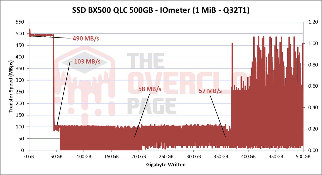
Although the writes to the target SSD are initially nearly 500 MB/s, the moment the ~45 GB pSLC cache fills up, the write speeds are reduced to the write speeds of the underlying Micron 3D QLC NAND, which are around 50 MB/s. Effectively QLC NAND Flash is no faster than a mechanical HDD, and with worse data retention and endurance characteristics. Clearly this is the point where the prophesied solid state storage future comes crumbling down as even relatively cheap NAND Flash still hasn’t caught up to the price/performance of HDDs.
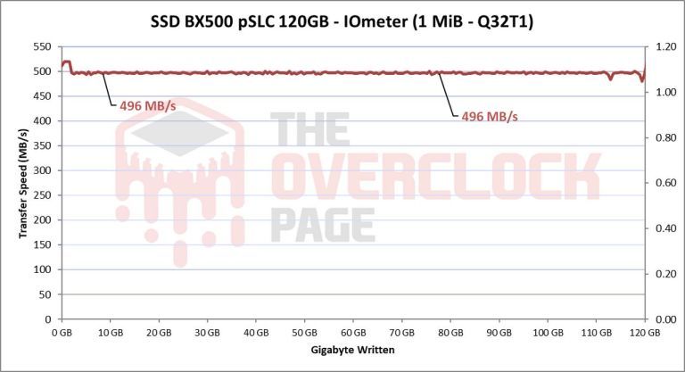
The modification performed by Gabriel Ferraz on the BX500 SSD involves reprogramming its Silicon Motion SM2259XT2 NAND Flash controller using the MPTools software, which is not provided to consumers but has been leaked onto the internet. While not as simple as toggling on a ‘use whole SSD as pSLC’ option, this is ultimately what it comes down to after flashing modified firmware to the drive.
With the BX500 SSD now running in pSLC mode, it knocks the storage capacity down from 500 GB to 120 GB, but the P/E rating goes up from a rated 900 cycles in QLC mode to 60,000 cycles in pSLC mode, or well over 3,000%. The write performance is a sustained 496 MB/s with none of the spikes seen in QLC mode, leading to about double the score in the PCMark 10 Full System Drive test.
With all of this in mind, it’s not easy to see a path forward for NAND Flash which will not make these existing issues even worse. Perhaps Intel and Micron will come out of left field before long with a new take on the 3D XPoint phase-change memory, or perhaps we’ll just keep muddling on for the foreseeable future with ever worse SSDs and seemingly immortal HDDs.
Clearly one should never believe prophets, especially not those for shiny futuristic technologies.
Featured image: “OCZ Agility 3 PCB” by [Ordercrazy]