Vista Normal

Hay nuevos artículos disponibles. Pincha para refrescar la página.
AnteayerSalida Principal

Chase Light SAO Shouldn’t Have Used a 555, and Didn’t

27 Marzo 2025 at 11:00

Around these parts, projects needlessly using a microcontroller where a simpler design would do are often derided with the catch-all “Should have used a 555,” even if the venerable timer chip wouldn’t have been the ideal solution. But the sentiment stands that a solution more complicated than it needs to be is probably one that needs rethinking, as this completely mechanical chaser light badge Simple Add-On (SAO) aptly demonstrates.

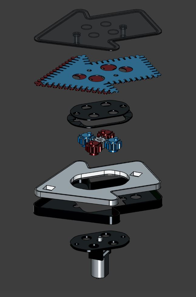
Rather than choosing any number of circuits to turn a strip of discrete lights on and off, [Johannes] took inspiration for his chaser lights from factory automation mechanisms that move parts between levels on steps that move out of phase with each other, similar to the marble-raising mechanism used in [Wintergatan]’s Marble Machine X.

Two thin plates with notches around the edge are sandwiched together inside the 3D printed case of the SAO, between the face and the light source. A small motor and a series of gears rotate the two masks 180° out of phase with each other, which creates the illusion that the light is moving.

It’s pretty convincing; when we first saw the video below, we were sure it was a row of tiny LEDs around the edge of the badge.

Hats off to [Johannes] for coming up with such a clever mechanism and getting it working just in time for Hackaday Europe. If you need to catch up on the talks, we’ve got a playlist ready for you.

Pulsed Deposition Points a Different Path to DIY Semiconductors

20 Febrero 2025 at 03:00

While not impossible, replicating the machines and processes of a modern semiconductor fab is a pretty steep climb for the home gamer. Sure, we’ve seen it done, but nanoscale photolithography is a demanding process that discourages the DIYer at every turn. So if you want to make semiconductors at home, it might be best to change the rules a little and give something like this pulsed laser deposition prototyping apparatus a try.

Rather than building up a semiconductor by depositing layers of material onto a silicon substrate and selectively etching features into them with photolithography, [Sebastián Elgueta]’s chips will be made by adding materials in their final shape, with no etching required. The heart of the process is a multi-material pulsed laser deposition chamber, which uses an Nd:YAG laser to ablate one of six materials held on a rotating turret, creating a plasma that can be deposited onto a silicon substrate. Layers can either be a single material or, with the turret rapidly switched between different targets, a mix of multiple materials. The chamber is also equipped with valves for admitting different gases, such as oxygen when insulating layers of metal oxides need to be deposited. To create features, a pattern etched into a continuous web of aluminum foil by a second laser is used as a mask. When a new mask is needed, a fresh area of the foil is rolled into position over the substrate; this keeps the patterns in perfect alignment.

We’ve noticed regular updates on this project, so it’s under active development. [Sebastián]’s most recent improvements to the setup have involved adding electronics inside the chamber, including a resistive heater to warm the substrate before deposition and a quartz crystal microbalance to measure the amount of material being deposited. We’re eager to see what else he comes up with, especially when those first chips roll off the line. Until then, we’ll just have to look back at some of [Sam Zeloof]’s DIY semiconductors.

❌
❌