Vista Normal

Hay nuevos artículos disponibles. Pincha para refrescar la página.
AnteayerSalida Principal

I2C For Hackers: The Basics

7 Agosto 2024 at 14:00

You only really need two data wires to transfer a ton of data. Standards like UART, USB2, I2C, SPI, PS/2, CAN, RS232, SWD (an interface to program MCUs), RS485, DMX, and many others, all are a testament to that. In particular, I2C is such a powerful standard, it’s nigh omnipresent – if you were to somehow develop an allergy to I2C, you would die.

Chances are, whatever device you’re using right now, there’s multiple I2C buses actively involved in you reading this article. Your phone’s touchscreen is likely to use I2C, so is your laptop touchpad, most display standards use I2C, and power management chips are connected over I2C more often than not, so you’re covered even if you’re reading this on a Raspberry Pi! Basically everything “smart” has an I2C port, and if it doesn’t, you can likely imitate it with just two GPIOs.

If you’re building a cool board with a MCU, you should likely plan for having an I2C interface exposed. With it, you can add an LCD screen with a respectable resolution or a LED matrix, or a GPS module, a full-sized keyboard or a touchpad, a gesture sensor, or a 9 degree of freedom IMU – Inertial Measurement Unit, like a accelerometer+compass+gyroscope combination. A small I2C chip can help you get more GPIOs for your MCU or CPU, or a multi-channel motor driver, or a thermal camera, or a heap of flash memory; if you’re adding some sort of cool chip onto your board, it likely has an I2C interface to let you fine-tune its fancy bits.

As usual, you might have heard of I2C, and we sure keep talking about it on Hackaday! There’s a good few long-form articles about it too, both general summaries and cool tech highlights; this article is here to fill into some gaps and make implicit knowledge explicit, making sure you’re not missing out on everything that I2C offers and requires you to know!

Basics And Addressing

A common I2C EEPROM – you likely have a good few such chips within a dozen meter radius. By [Raimond Spekking], CC BY-SA 4.0
I2C is a two-wire interface, and you can put multiple devices on these two wires – thanks to an addressing system and strictly defined hierarchy. One party on the bus is the one always initiating all conversations (old: master, new: controller), and this role is basically always static; usually, it’s your MCU. Your devices can’t send data to your MCU on your own – your MCU has to read data from your devices. As such, you usually can’t make bidirectional effortless communications UART style, unless you dig deep enough to make “multi-master” communications work – which is a cool feature but is often poorly supported.

Instead, if your device is the kind you expect to return important data at random points, there’s often an INT pin – the INT pin is not included in the standard and usually is not required to use any I2C device, but if your IC or breakout exposes the INT pin, you should consider using it, since it will save you a fair bit of CPU time spent polling your device for data.

I2C is wonderful in that you can put a large number of devices on your bus – as long as your communications can physically stay stable. How does it work? Addresses. Devices are pre-programmed with an address you can use to talk to them, and you can query a bus to get a list of addresses that the connected devices respond on. Some devices can only have a single address so you can only add one of them to a – unless you hack it in one of the ways I’ll describe below. Many devices that – for instance, SSD1306 displays have a single pin you can tie high or low, so you can put two of these devices on the same bus, and GPIO expanders tend to have three pins that result in eight possible addresses. Rarely, there are devices that let you reprogram their address with a command, too.

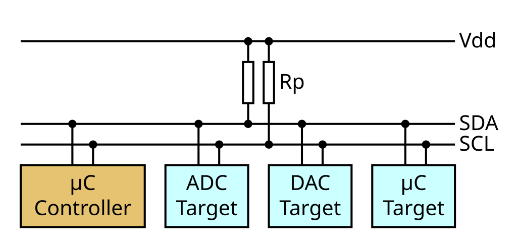
An I2C device’s address is specified in the datasheet. Beware – addresses are 7-bit, and during transfer, the address is shifted and the least significant bit signifies whether a write or read operation is happening; some datasheets will show the address in its proper 7-bit form and some show it already shifted. The way you can notice the latter if you see separate read and write addresses specified – that’s a non-shifted address. A surefire way is to connect your device to any I2C controller and scan for devices, of course. I2C addresses aren’t unique like MAC addresses, so, there’s way more kinds of I2C devices than there are addresses. Here’s a database you can check for fun, but it’s definitely incomplete. 10-bit addresses exist and they do widen the address space comfortably, but they’re still not that popular. Remember – an I2C bus can be scanned, and it’s a pretty wonderful feature – it gives you a sanity check showing that a device is connected, a check that you don’t really get with interfaces like SPI and UART!

An I2C device with a twist. ADDR here is set by connecting it to SCL/SDA/GND/VCC (4 bits with one pin), and, INT pin here is called ALERT. By [Pradeep717], CC BY-SA 4.0
How do you avoid address conflicts, in case you’re planning to use multiple devices? Plan ahead, use address changing pins where possible, and use tricks. There are chips that help you put more devices on an I2C bus, for instance, acting like a “gateway” – it’s a saturated market, with Linear Technology taking up a lot of its space with their famously pricy but seriously worthwhile ICs, and they even have Linux drivers! There’s also a large number of tricks – some hackers suggest using SCL lines as chip selects, some suggest swapping SCL and SDA, and some talk about powering devices down selectively; if you’re experiencing address conflicts, you won’t be able to solve this purely in software, but it’s certain you won’t run out of hardware options.

Clocks And Pullups

There’s three standard I2C clock speeds – 100kHz, 400kHz and 1MHz, some hosts and devices can go even higher but it’s not especially prominent. Technically, you can go higher or lower, software I2C implementations often do, but some devices might not like it. Hosts often run at 100kHz, but it’s common that you can up the frequency and switch it into 400kHz; however, there’s hosts that are hardwired to 100kHz operation, like VGA/DVI/HDMI port and desktop/laptop-internal I2C controllers.

This affects, and sometimes, if you have choice between I2C and some other interface, speed might be a deciding factor. For example, take SSD1306 or SH1106 OLED screens – they can be connected through either I2C or SPI, so if you’re using a breakout, it just depends on the way it’s wired. You won’t be able to send data to an I2C screen as quickly over SPI, because of the inherent data cap – they supports SPI links at multiple MHz clock rate, whereas an I2C link will be limited to 400KHz. Want faster screen refresh? You’ll want to wire the screen into SPI mode. Fine with possibly lower FPS? I2C is a valid choice, then.

You need pullups – and you cannot use GPIO-internal pullups like you can do with buttons, they are too high of a value as a rule. A typical range for a pullup is from 1K to 10K – going too high will distort the signal on the bus, and going too low will make the bus impossible to drive. Raspberry Pi boards use 1.8K pullups on the dedicated I2C bus, 4.7K is another popular value, and I’ve had 10K pullups result in unstable communications at higher speeds, so I typically go lower a fair bit, using 1.8K, 4.7K or 5.1K pullups. Mind you, if both your device, so if an I2C sensor breakout is failing to respond when connected to a Raspberry Pi but it really should work, check whether you maybe should desolder or disconnect the pullups on the sensor board itself.

I2C is pretty cool indeed – all those devices I mentioned in the intro, they’re a breakout board and a cable away, often, you don’t even have to solder. Looking to use I2C on your board as an expansion interface, but don’t know what kind of connector to use? It’s pretty simple, I’ve talked about it in my article on I2C ecosystems. One five-pin header and one four-pin JST-SH is all you need, and you can even get vertical JST-SH connectors if space is a concern!

Next time, let’s talk more about I2C devices, the kinds of I2C interfaces you will encounter and all the places they are usually hidden in, types of I2C transfers you can do, and notable implementation nuances, – leaving no stone unturned as usual.

Secrets of the Old Digital Design Titans

18 Julio 2024 at 14:00

Designing combinatorial digital circuits seems like it should be easy. After all, you can do everything you want with just AND, OR, and NOT gates. Bonus points if you have an XOR gate, but you can build everything you need for combinatorial logic with just those three components. If all you want to do is design something to turn on the light when the ignition is on AND door 1 is open OR door 2 is open, you won’t have any problems. However, for more complex scenarios, how we do things has changed several times.

In the old days, you’d just design the tubes or transistor circuits you needed to develop your logic. If you were wiring up everything by hand anyway, you might as well. But then came modules like printed circuit boards. There was a certain economy to having cards that had, say, two NOR gates on a card. Then, you needed to convert all your logic to use NOR gates (or NAND gates, if that’s what you had).

Small-scale ICs changed that. It was easy to put a mix of gates on a card, although there was still some slight advantage to having cards full of the same kind of gate. Then came logic devices, which would eventually become FPGAs. They tend to have many of one kind of “cell” with plenty of logic gates on board, but not necessarily the ones you need. However, by that time, you could just tell a computer program what you wanted, and it would do the heavy lifting. That was a luxury early designers didn’t have.

Basis

How can you do everything with a NOR gate? Easy if you don’t mind spending gates. Obviously, if I need a NOR gate, I’m done. If I need an OR gate, I just feed the output of a NOR gate to all the pins of another NOR gate. The output of the second gate will be the OR of the first gate’s inputs.

DeMorgan’s theorem tells us that if NOT(A OR B) is the same as (NOT A) AND (NOT B). It is!

A B NOT A NOT B NOT(A OR B) (NOT A) AND (NOT B)
0 0 1 1 1 1
0 1 1 0 0 0
1 0 0 1 0 0
1 1 0 0 0 0

So you can create a NOT gate with a NOR gate (or a NAND gate) and an AND/NAND gate by mixing up NOR and NOT gates. Conversely, you can create OR/NOR gates by mixing up NAND and NOT gates. So, either way, you are covered.

The only problem is figuring out how to express any arbitrary expression as a bunch of NOR or NAND gates. A common way to do this is to have a “product of sums” or “sum of products” arrangement. In this context, a product is an AND gate, and a sum is an OR gate. This also works with things where you use diodes and wired AND logic, such as those you find in a programmable logic array or open collector arrangements. Think about it. A bunch of open collector outputs tied to a pull up resistor acts like a giant AND gate. Any low input causes a low output.

Suppose you wanted to determine whether a two-bit binary number is odd or even. Yes, yes, there is an easy way to do that, but assume you don’t know that yet. Let’s assume the most significant bit is A and the least significant is B. Further, we’ll use the notation A’ for NOT(A). AB is A AND B, while A+B is A OR B. The two odd values are 01 and 11, so we can set up another logical Y that is true when we have one of those OR the other:

Y=A'B + AB

Troubleshooting

This works, of course. But if you are adept at troubleshooting digital logic, you might notice something — again, assuming that you don’t already know the answer to this problem. The output, Y, doesn’t really depend on A at all because we have A’B or AB together. So just intuitively, we know the real answer is Y=B. No gates are needed at all!

But how would we figure out a minimum in a more complex example? For instance, suppose you have a four-digit number and want to drive a seven-segment LED. Segment a, for example, is the top bar of the figure 8 that forms the display. It should be on for inputs 0, 2, 3, 5, 6, 7, 8, and 9. Then, you need to do this for six other segments. Hard to see exactly how to decode that, right?

Methods

Before computers would do it for you, there were two common methods to resolve things like this without resorting to brute force. The most notable of these is the Karnaugh or K map. These are great for a small number of inputs. Let’s go back to the two-bit number. Our K map looks like this one.

A two-input K map

Each of these four cells containing a zero or one represents a single AND gate with A and B set as shown (that is, if A or B are true or false). The number in the cell is the output in that state. If you don’t care about an output given a certain state of inputs, you can put an X in that square and treat them the same as a 1 if you want to (but you don’t have to). By the way, these maps were made using the very useful K map solver you can find online.

Next, you circle all the 1’s that are next to each other in a rectangle including any that wrap around the edges. When you have a bunch of ones clustered together, you can wipe out the variables that change from 0 to 1 in the group.

In this case, the 1’s cover both A and A’, so we can easily see the answer is Y=B. Of course, we knew that already, but you can figure it out easily using a map like this, even if you don’t already know the answer.

For a map this small, you don’t have many options, but the number of 1s (or Xs) in an implicant — a group — must be a power of two. So you can draw a rectangle around two cells or four, but not three.

Bigger, My My…

A 3-input K map

Note that the values of A and B only change by one bit in adjacent cells. So, a 3-variable K map looks like this is the one adjacent. Note that the left-hand column reading from top to bottom goes 00, 01, 11, 10. So, only one bit changes at a time (like a grey code).

In this case, the prime implicants — the parts that matter — are A’B’ and B’C’. That’s because the top row strikes the C input when AB=00 and the top left 1 and the bottom left 1 join to cancel out A.

Two implicants: A’B’ and B’C’

Every rectangular grouping that covers a power of two cells is a prime implicant. Sometimes, a group will cover terms that other groups will also cover. In that case, that group is not an essential prime implicant but, rather, a redundant prime implicant. But if even one square only belongs to a group, then that group is an essential prime implicant and will have a role in the final result. Sometimes, you’ll have several prime implicants that cover each other so that you can pick one or the other, and it doesn’t matter which one. Those are known as selective prime implicants.

As you can see below, once you have four bits, the K map gets large. Beyond 4 bits, it is usually impractical without switching how you draw the map. Remember the 7-segment decoder example? Here is the K map for segment A of a decoder that accepts numbers from 0 to 9. Note the Xs for numbers larger than 9. If you draw circles around the groupings of 1s, you can develop the formula: Y=C+A +B’D’+BD. That’s much easier than trying to do it without a K map. The C is due to the right-hand columns (remember to include the Xs when it helps you). The A term is due to the bottom two rows. The other two terms pick up the stray 1’s not covered by those two groups. Of course, to design an entire decoder, you’d need six more K maps, one for each segment.

It is also possible to group the 0s instead of the 1s and obtain a product of sums. The process is similar but you use the 0’s and not the 1’s.

The real challenge is when you want to go beyond four bits. For that, you often go to a table-like format known as the Quine McCluskey method. Or just use a computer. We won’t judge.

Of course, if you want to make complex digital designs, you need a clock. But you can still use maps where you need combinatorial logic in a synchronous design. We mentioned you can make anything out of AND, OR, and NOT. But you can get those gates using a multiplexer or even a relay, which is, after all, just a mechanical multiplexer. Come to think of it, you can make logic gates out of darn near anything.

Banner image by [Kit Ostrihon], demonstrating multidimensional K-maps

Thumbnail image: “K-map 6,8,9,10,11,12,13,14 anti-race” by [Cburnett]


Embedded Python: MicroPython Is Amazing

11 Julio 2024 at 14:00

In case you haven’t heard, about a month ago MicroPython has celebrated its 11th birthday. I was lucky that I was able to start hacking with it soon after pyboards have shipped – the first tech talk I remember giving was about MicroPython, and that talk was how I got into the hackerspace I subsequently spent years in. Since then, MicroPython been a staple in my projects, workshops, and hacking forays.

If you’re friends with Python or you’re willing to learn, you might just enjoy it a lot too. What’s more, MicroPython is an invaluable addition to a hacker’s toolkit, and I’d like to show you why.

Hacking At Keypress Speed

Got a MicroPython-capable chip? Chances are, MicroPython will serve you well in a number of ways that you wouldn’t expect. Here’s a shining example of what you can do. Flash MicroPython onto your board – I’ll use a RP2040 board like a Pi Pico. For a Pico, connect an I2C device to your board with SDA on pin 0 and SCL on pin 1, open a serial terminal of your choice and type this in:

>>> from machine import I2C, Pin
>>> i2c = I2C(0, sda=Pin(0), scl=Pin(1))
>>> i2c.scan()

This interactivity is known as REPL – Read, Evaluate, Print, Loop. The REPL alone makes MicroPython amazing for board bringup, building devices quickly, reverse-engineering, debugging device library problems and code, prototyping code snippets, writing test code and a good few other things. You can explore your MCU and its peripherals at lightning speed, from inside the MCU.

When I get a new I2C device to play with, the first thing I tend to do is wiring it up to a MicroPython-powered board, and poking at its registers. It’s as simple as this:

>>> for i in range(16):
>>>     # read out registers 0-15
>>>     # print "address value" for each
>>>     print(hex(i), i2c.readfrom_mem(0x22, i))
>>> # write something to a second (0x01) register
>>> i2c.writeto_mem(0x22, 0x01, bytes([0x01]) )

That i2c.scan() line alone replaces an I2C scanner program you’d otherwise have to upload into your MCU of choice, and you can run it within three to five seconds. Got Micropython running? Use serial terminal, Ctrl+C, and that will drop you into a REPL, just type i2c.scan() and press Enter. What’s more, you can inspect your code’s variables from the REPL, and if you structure your code well, even restart your code from where it left off! This is simply amazing for debugging code crashes, rare problems, and bugs like “it stops running after 20 days of uptime”. In many important ways, this removes the need for a debugger – you can now use your MCU to debug your code from the inside.

Oh, again, that i2c.scan()? You can quickly modify it if you need to add features on the fly. Want addresses printed in hex? (hex(addr) for addr in i2c.scan()). Want to scan your bus while you’re poking your cabling looking for a faulty wire? Put the scan into a while True: and Ctrl+C when you’re done. When using a typical compiled language, this sort of tinkering requires an edit-compile-flash-connect-repeat cycle, taking about a dozen seconds each time you make a tiny change. MicroPython lets you hack at the speed of your keyboard typing. Confused the pins? Press the `up` button, edit the line and run the i2c = line anew.

To be clear, all of code is running on your microcontroller, you just type it into your chip’s RAM and it is executed by your MCU. Here’s how you check GPIOs on your Pi Pico, in case you’re worried that some of them have burnt out:

>>> from machine import Pin
>>> from time import sleep
>>> pin_nums = range(30) # 0 to 29
>>> # all pins by default - remove the ones connected to something else if needed
>>> pins = [Pin(num, Pin.OUT) for num in pin_nums]
>>> 
>>> while True:
>>>   # turn all pins on
>>>   for i in range(len(pins)):
>>>     pins[i].value(True)
>>>   sleep(1)
>>>   # turn all pins off
>>>   for i in range(len(pins)):
>>>     pins[i].value(False)
>>>   sleep(1)
>>>   # probe each pin with your multimeter and check that each pin changes its state

There’s many things that make MicroPython a killer interpreter for your MCU. It’s not just the hardware abstraction layer (HAL), but it’s also the HAL because moving your code from board to board is generally as simple as changing pin definitions. But it’s all the other libraries that you get for free that make Python awesome on a microcontroller.

Batteries Included

It really is about the batteries – all the libraries that the stock interpreter brings you, and many more that you can download. Only an import away are time, socket, json, requests, select, re and many more, and overwhelmingly, they work the same as CPython. You can do the same r = requests.get("https://retro.hackaday.com"); print(r.text)[:1024] as you would do on desktop Python, as long as you got a network connection going on. There will be a few changes – for instance, time.time() is an integer, not a float, so if you need to keep track of time very granularly, there are different functions you can use.

Say, you want to parse JSON from a web endpoint. If you’re doing that in an Arduino environment, chances are, you will be limited in what you can do, and you will get triangle bracket errors if you mis-use the JSON library constructs because somehow the library uses templates; runtime error messages are up to you to implement. If you parse JSON on MicroPython and you expect a dict but get a list in runtime, it prints a readable error message. If you run out of memory, you get a very readable MemoryError printed out, you can expect it and protect yourself from it, even fix things from REPL and re-run the code if needed.

The user-supplied code is pretty good, too. If you want PIO or USB-HID on the RP2040, or ESP-CPU-specific functions on the ESP family, they are exposed in handy libraries. If you want a library to drive a display, it likely already has been implemented by someone and put on GitHub. And, if that doesn’t exist, you port one from Arduino and publish it; chances are, it will be shorter and easier to read. Of course, MicroPython has problems. In fact, I’ve encountered a good few problems myself, and I would be amiss not mentioning them.

Mind The Scope

In my experience, the single biggest problem with MicroPython is that writing out `MicroPython` requires more of my attention span than I can afford. I personally shorten it to uPy or just upy, informally. Another problem is that the new, modernized MicroPython logo has no sources or high-res images available, so I can’t print my own stickers of it, and MicroPython didn’t visit FOSDEM this year, so I couldn’t replenish my sticker stock.

On a more serious note, MicroPython as a language has a wide scope of where you can use it; sometimes, it won’t work for you. An ATMega328P can’t handle it – but an ESP8266 or ESP32 will easily, without a worry in the world, and you get WiFi for free. If you want to exactly control what your hardware does, counting clock cycles or hitting performance issues, MicroPython might not work for you – unless you write some Viper code.

If you want to have an extremely-low-power MCU that runs off something like energy harvesting, MicroPython might not work – probably. If you need your code run instantly once your MCU gets power, mind the interpreter takes a small bit of time to initialize – about one second, in my experience. If you want to do HDMI output on a RP2040, perhaps stick to C – though you can still do PIO code, there are some nice libraries for it.

Some amount of clock cycles will be spent on niceties that Python brings. Need more performance? There are things you can do. For instance, if you have a color display connected over SPI and you want to reduce frame rendering time, you might want to drop down to C, but you don’t have to ditch MicroPython – just put more of your intensive code into C-written device drivers or modules you compile, and, prototype it in MicroPython before you write it.

As Seen On Hackaday

If you’ve followed the USB-C PD talking series, you must’ve seen that the code was written in MicroPython, and I’ve added features like PD sniffing, DisplayPort handling and PSU mode as if effortlessly; it was just that easy to add them and more. I started with the REPL, a FUSB302 connected to a RP2040, poking at registers and reading the datasheet, and while I needed outside help, the REPL work was so so much fun!

There’s something immensely satisfying about poking at a piece of technology interactively and trying to squeeze features out of it, much more if it ends up working, which it didn’t, but it did many other times! I’ve been hacking on that PD stack, and now I’m slowly reformatting it from a bundle of functions into object-based code – Python makes that a breeze.

Remember the Sony Vaio board? Its EC (embedded controller) is a RP2040, always powered on as long as batteries are inserted, and it’s going to be running MicroPython. The EC tasks include power management, being a HID over I2C peripheral, button and LED control, and possibly forwarding keyboard and trackpoint events to save a USB port from the second RP2040, which will run QMK and server as a keyboard controller. MicroPython allows me to make the firmware quickly, adorn it with a dozen features while I do it, and keep the codebase expandable on a whim. The firmware implementation will be a fun journey, and I hope I can tell about it at some point.

Have you used MicroPython in your projects? What did it bring to your party?

PCB Design Review: HAB Tracker With ATMega328P

10 Julio 2024 at 14:20

Welcome to the Design Review Central! [VE3SVF] sends us their board, and it’s a HAB (High Altitude Balloon) tracker board. It’s got the venerable ATMega28P on it, a LoRa modem and a GPS module, and it can be powered from a LiIon battery. Stick this board with its battery onto a high-altitude balloon, have it wake up and transmit your coordinates every once in a while, and eventually you’ll find it in a field – if you’re lucky. Oherwise, it will get stuck hanging on a tree branch, and you will have to use a quadcopter to try and get it down, and then, in all likelihood, a second quadcopter so that you can free the first one. Or go get a long ladder.

The ATMega328P is tried and true, and while it’s been rising in price, it’s still available – with even an updated version that sports a few more peripherals; most importantly, you’re sure to find a 328P in your drawer, if not multiple. Apart from that, the board uses two modules from a Chinese manufacturer, G-Nice, for both GPS and Lora. Both of these modules are cheap, making this tracker all that more accessible; I could easily see this project being sold as a “build your own beacon” kit!

Let’s make it maybe a little nicer, maybe a little cheaper, and maybe decrease the power consumption a tad along the way. We’ll use some of the old tricks, a few new ones, and talk about project-specific aspects that might be easy to miss.

The Low Hanging Fruit

Way better than the 0.5mm/0.25mm defaults, so make sure to replace them! Can even go down to 0.17mm if called for.

This board has four layers, which is nice because you get more ground and more routing space for a tiny price increase these days. This board doesn’t add fills on inner layers, but that is an easy fix – just select one of the GND power planes and tick the In1/In2.Cu boxes in their settings. Another thing to tweak in zone settings is zone clearance and minimum thickness – default KiCad clearances are way too conservative, setting them to something like 0.2 mm / 0.2 mm is a good idea. That improves ground connectivity, and also lets us get rid of ground tracks that would otherwise be necessary to bring ground to different connectors.

The inner layers have ground, and ground on all layers can reach further, too. That said, the inner layers benefit from being completely free – that’s when you get the best return current flow. Remember, each track, whether signal or power, needs its ground return path, and if you don’t provide a direct clean one, electricity will find a way. That, in turn, results in noise, both received and emitted, as well as possible instabilities.

In particular, the ISP flashing header had a lot of low-hanging fruit; tracks that were pulled on inner layers but could as well go on top/bottom layers. Many tracks could be snaked between GPS and LoRa module pads, too – the gaps are wide enough, that even a 0.2 mm track feels comfortable in there, and you could probably pull two if you dropped down to 0.15 mm, which is still safe with most fabs.

And, after a dozen minutes of work, the inner layers are free. A surprising amount of space could be found – for instance, the three DIO tracks nicely went along the right edge of the board. More importantly, capacitors were moved closer to where they work best. In particular, the AREF capacitor is two vias and one long inner track apart, which won’t make for good analog decoupling. That did require moving the ATMega a bit upwards, but a judicious application of Del and Shift+Del on tracks, as well as some track dragging, made that move go quickly.

I could talk about component size choices, but they’re not meaningfully interfering with routing on the board – even the opposite, having one of the diodes be 1206 helps me avoid some vias. On the other hand, rotating the battery divider resistors and power regulators 180 degrees resulted in some good routing space freed up. And, looking at the board, the ATMega328P routing could perhaps use being rotated one turn clockwise, too. That’d make SPI routing cleaner, power tracks and analog pins shorter, and let us put capacitors at the sides, at the low low cost of having GPIO pins snake around a bit. However, here, the benefits aren’t necessarily as clear-cut as in previous articles; instead, it’s a time vs niceness tradeoff.

The Chip Gets Rotated, But Not Necessarily

Here, a conundrum. We could spend maybe a dozen more minutes and rotate the chip, or leave it be? Is the board going to be slightly nicer? Yes. Is this necessary? No. If you want to just order the board and go, it’s completely fair for you to press order and leave improvements of this grade for rev2. On the other hand, if the itch to improve your board is bad enough that the time investment doesn’t scare you out of it, give in and see yourself become better at PCB design. Worked for me.

There are hidden problems for such small redesigns, though. Remember, a redesign might have you reinstate a problem that you’ve successfully avoided with the original iteration, or, it can quickly become infeasible. I’ve had it happen, where a redesign that intended to add features and reduce complexity has become counter-productive midway through, so, I’ve had to stop myself from continuing and just order the board already. You’ll learn to keep track of these, but it does take keeping it in mind. Keep your Ctrl+Z’s ready, keep a copy of the files, or a Git commit, if you are doing something fundamental, and be ready to get a lesson in letting go.

I ended up rotating the chip, and the board did indeed become a bit nicer, but in ways that don’t solve any pressing problems. By the way, have you noticed something this board has done really well from the start? That’s component placement. The ways the LoRa module, GPS module, ATMega328P and the headers are positioned, I wouldn’t change anything about them. Maybe move the pin headers onto a 2.5 4mm grid so that you could expand this board with a perfboard if needed, but that one isn’t a must – this is a low weight board, after all, the headers are more for debugging than anything else.

Last Thoughts: Inner Layers And Antenna Choice

If you have internal layers, use them for ground or power fills, so that power and return currents can flow unrestricted. This is going to reduce both radiated and received emissions, as well as make power rails smoother, which feels mighty helpful considering this design has two radios on it and the GPS radio has a passive antenna.

Also, some fabs don’t want empty inner layers. Last year, JLCPCB started refusing boards with inner or outer layers more than 30% full, in what’s presumably an attempt to decrease the etching process costs, causing some people to redesign perfectly working PCBs with little notice. Combine this with a recent documentation overhaul that just so happened to turn some previously free options into paid ones, and if I were to guess, they are no longer able to keep running at a loss as much as they did, so, the age of golden offers at JLCPCB might soon to be over.

Our improvements ended up providing more than enough copper on top and bottom layers, that you could possibly switch this board to two-layer; again, cheaper ordering, possibly quicker manufacturing time, possibly cheaper PCBA. Isn’t a requirement, but it is nice when you can do it. If you are to keep the two extra layers, remember that on-board antennas need keepouts at least for a wide patch under them, if not for a good amount of space around them, and the keepout has to be on all layers. No tracks, no fills, no copper, do not pass go, do not collect 200.

Thicker tracks for power paths are good whenever you can afford them – and this board has plenty of space! I personally usually add them in last, and it’s not a problem here, but it’s most certainly a smarter decision to draw them thick first so that you don’t have to do a re-layout later.

It also does feel like you could consider an active antenna here. For a high-altitude balloon, sure, you’re way way more likely to get a fix and you’ve got a whole lot more time to do it, but I would guess improving your chances is worthwhile. Plus, I don’t know much about G-Nice’s modules, still yet to try out the one I purchased last year – it might be that this module is perfectly okay, but it concerns me these are meant to be footprint-compatible drop-in replacements for well-established company modules, with this specific module borrowing an U-Blox footprint, and as such, I don’t know how much to expect. An active antenna adds a fair of weight and size footprint, and it might be that everyone’s flying with passive antennas no worries, so I might be completely out of my zone here. Whichever is the case, I would appreciate input!

As usual, if you would like a design review for your board, submit a tip to us with [design review] in the title, linking to your board files. KiCad design files strongly preferred, both repository-stored files (GitHub/GitLab/etc) and shady Google Drive/Dropbox/etc .zip links are accepted.

Digital Skills: Artificial Intelligence by Accenture

Por: EasyWithAI
19 Julio 2023 at 04:30
Category – General Artificial Intelligence Course Difficulty – Easy Course Length – 3 Weeks / 6 Hours Price – Free Rating  4.5/5 View Course Discover the potential for artificial intelligence to transform everyday life and reshape the way you work in this comprehensive online course from Accenture. With a duration of 3 weeks and […]

Source

❌
❌