Summer has settled upon the northern hemisphere, which means that it’s time for sweet, sweet strawberries to be cheap and plentiful. But would you believe they taste even better in freeze-dried format? I wouldn’t have ever known until I happened to get on a health kick and was looking for new things to eat. I’m not sure I could have picked a more expensive snack, but that’s why we’re here — I wanted to start freeze-drying my own strawberries.
While I could have just dropped a couple grand and bought some kind of freeze-drying contraption, I just don’t have that kind of money. And besides, no good Hackaday article would have come out of that. So I started looking for alternative ways of getting the job done.
Early on in my web crawling on the topic, I came across this Valley Food Storage blog entry that seems to have just about all the information I could possibly want about the various methods of freeze-drying food. The one that caught my eye was the dry ice method, mostly because it’s only supposed to take 24 hours.
Here’s what you do, in a nutshell: wash, hull, and slice the strawberries, then put them in a resealable bag. Leave the bag open so the moisture can evaporate. Put these bags in the bottom of a large Styrofoam cooler, and lay the dry ice on top. Loosely affix the lid and wait 24 hours for the magic to happen.
I still had some questions. Does all the moisture simply evaporate? Or will there be a puddle at the bottom of the cooler that could threaten my tangy, crispy strawberries? One important question: should I break up the dry ice? My local grocer sells it in five-pound blocks, according to their site. The freeze-drying blog suggests doing a pound-for-pound match-up of fruit and dry ice, so I guess I’m freeze-drying five entire pounds of strawberries. Hopefully, this works out and I have tasty treats for a couple of weeks or months.
Preparation
In order to make this go as smoothly as possible, I bought both a strawberry huller and a combination fruit and egg slicer. Five pounds of strawberries is kind of a lot, eh? I’m thinking maybe I will break up the ice and try doing fewer strawberries in case it’s a complete failure.
I must have gotten rid of all our Styrofoam coolers, so I called the grocery store to make sure they have them. Unfortunately, my regular store doesn’t also have dry ice, but that’s okay — I kind of want to be ready with my cooler when I get the dry ice and not have to negotiate buying both while also handling the ice.
So my plan is to go out and get the cooler and the strawberries, then come back and wash the berries. Then I’ll go back out and get the dry ice and then hull and slice all the berries. In the meantime, I bought some food-safe desiccant packets that absorb moisture and change color. If this experiment works, I don’t want my crispy strawberries ruined by Midwestern humidity.
Actually Doing the Thing
So I went and bought the cooler and the strawberries. They were $2.99 for a 2 lb. box, so I bought two boxes, thinking that a little more poundage in dry ice than berries would be a good thing. I went back out to the other grocery store for the dry ice, and the person in the meat department told me they sell it in pellets now, in 3- and 6-lb. bags. So I asked for the latter. All that worrying about breaking it up for nothing!
Then it was go time. I got out my cutting board and resigned myself to hulling and slicing around 75 strawberries. But you know, it really didn’t take that long, especially once I got a rhythm going. I had no idea what the volume would be like, so I started throwing the slices into a gallon-sized bag. But then it seemed like too much mass, so I ended up with them spread across five quart-sized bags. I laid them in the bottom of the cooler in layers, and poured the dry ice pellets on top. Then I took the cooler down to the basement and made note of the time.
Since I ended up with six pounds of dry ice and only four pounds of strawberries, my intent is to check on things after 18 hours, even though it’s supposed to take 24. My concern is that the strawberries will get done drying out earlier than the 24-hour mark, and then start absorbing moisture from the air.
Fruits of Labor
I decided to check the strawberries a little early. There was no way the ice was going to last 24 hours, and I think it’s because I purposely put the lid on upside down to make it extra loose. The strawberries are almost frozen and are quite tasty, but they are nowhere near depleted of moisture. So I decided to get more ice and keep going with the experiment.
I went out and got another 6 lb. of pellets. This time, I layered everything, starting with ice in the bottom and ending with ice on top. This time, I put the lid on the right way, just loosely.
Totally Not Dry, But Tasty
Well, I checked them a few hours before the 24-hour mark, and the result looks much the same as the previous morning. Very cold berries that appear to have lost no moisture at all. They taste great, though, so I put them in the freezer to use in smoothies.
All in all, I would say that this was a good experiment. Considering I didn’t have anything I needed when I started out, I would say it was fairly cost-effective as well. Here’s how the pricing breaks down:
28-quart Styrofoam cooler: $4.99
4 lbs. of strawberries: $5.99
12 lbs. of dry ice at $1.99/lb.: $24
a couple of resealable bags: $1
Total: $36, which is a little more than I paid for a big canister of freeze-dried strawberries on Amazon that lasted maybe a week. If this had worked, it would have been pretty cost-effective compared with buying them.
So, can you freeze-dry strawberries without a machine? Signs still point to yes, but I’m going to go ahead and blame the Midwestern humidity on this one. You can bet I’ll be trying this again in the winter, probably with fewer berries and smaller cooler. By the way, there was a small puddle underneath the cooler when it was all said and done.
Have you ever tried freeze-drying anything with dry ice? If so, how did it go? Do you have any tips? Let us know in the comments.
Do you have a 5 V device you want to run 24/7, no matter whether you have electricity? Not to worry – Linear Technology has made a perfect IC for you, the LTC4040; with the perfect assortment of features, except perhaps for the hefty price tag.
[Lukilukeskywalker] has shared a PCB for us to review – a LTC4040-based stamp you can drop onto your PCB whenever you want a LTC4040 design. It’s a really nice module to see designed – things like LiFePO4 support make this IC a perfect solution for many hacker usecases. For instance, are you designing a custom Pi HAT? Drop this module to give your HAT the UPS capability for barely any PCB effort. if your Pi or any other single-board computer needs just a little bit of custom sauce, this module spices it up alright!
This one is a well-designed module! I almost feel like producing a couple of these, just to make sure I have them handy. If you like the LTC4040, given its numerous features and all, this is also not the only board in town – here’s yet another LTC4040 board that has two 18650 holders, and referencing its PCBdesign will help me today in this review, you can take a look at it too!
Now, having looked at this PCB for a fair bit, it has a few things that we really do want to take care of. Part of today’s review will be connector selection, another would be the module form-factor, some layout, and some suggestions on sizing the passives – the rows of 1206 components are pretty, but they’re also potentially a problem. Let’s waste no time and delve in.
Battery Wireup And Formfactor
The battery connector uses JST-SH, one pin for VBAT and one for GND. The problem with this is that the module is capable of 2.5 A at 5 V = 12 W. At 3.6 V, that’s 4 A if not more and JST-SH is only rated for 1 A per pin. Using this module with a battery as-intended will melt things. You could add a bigger connector like the standard JST-PH, but that’d increase the module size, and my assessment is that this board doesn’t have to be larger than it already is.
Thankfully, this is an open-source module, so we can change its pinout easily enough, adding pins for the battery into the mix. Currently, this board feels breadboardable, but it isn’t quite – it’s pretty wide, so it will take two breadboards to handle, and a breadboard would also probably be disappointed with the pin amount required. With that in mind, adding pins at the top looks convenient enough.
In general, shuffling the pins around will help a fair bit. My hunch is to make the module’s castellations asymmetric, say, do 7-5-5-5 – one side with seven pins, three sides with five pins. It might not look as perfect, but what’s important is that it will be way way harder to mount incorrectly, something I’ve done with a module of my own design – that was not fun to fix. If you are worried about having enough pins to fill the resulting 22-pin combination, it’s always great to just add GND, doubly so for a power-related module!
Adding more castellations also helps us shuffle the pinout around, freeing up the routing – let’s go through the pins and see what that could help with.
Pinout Changes
The schematic is seriously nice looking – every single block is nicely framed and has its description listed neatly. Comparing it with reference schematic, it looks pretty good!
There’s a few nits to pick. For instance, BST_OFF and CHG_OFF need to be grounded for the IC to work – datasheet page 10. You could ground them through a resistor and pull them onto a castellation, but you can’t leave them floating. This is not easy to notice, however, unless you go through the pins one by one and recheck their wiring; I noticed it because I was looking at the board, saw two unconnected pins and decided to check.
My hunch is that, first, all the pins were given power names, and then two of them were missed as not connected anywhere, which is an understandable mistake to make.
Let’s keep with the schematic style – add two more connectors, one 5-pin and one 7-pin, rearrange the pinout, and keep them in their own nicely delineated area. The 7-pin connector gets the battery pins and a healthy dose of ground, and as for the 5 extra pins at the bottom, they’ll serve as extra ground pins, and give us shuffling slots for pins that are best routed southward.
Components And Placement
Having 1206 resistors on such a module is a double-edged sword. On one hand, given the adjustability, you definitely want resistors that you’d be able to replace easily, so 0402 is not a great option. However, 1206 can actually be harder to replace with a soldering iron, since you need to heat up both sides. The writing is more readable on 1206, no doubt, and it’s also nice that this module is optimized by size. Still, for the sake of routability, I will start by replacing the LEDs and LED resistors with 0603 components – those are resistors you will not be expected to replace, anyway.
Also, I have a hunch that a few components need to be moved around. First one is the RProg, no doubt – it’s in the way of the switching path, going right under the SW polygon. Then, I will rotate the Rsense resistor so that it’s oriented vertically – it feels like that should make the VIN track less awkward, and show whether there’s any space to be freed on the left.
Resistors replaced, a few components moved, and here’s where the fun begins. The IGATE track is specifically designated in the datasheet as pretty sensitive, to the point the PDF talks about leakage from this track to the other tracks – it is a FET gate driver output, after all. Having it snake all around power tracks feels uncomfortable I’d like to refactor these FETs a bit, and see if I can make the IGATE track a bit more straightforward, perhaps also make the space usage on the left more optimized. While doing that, I will be shuffling pins between the castellated edges every now and then.
After a bit of shuffling and component rerouting, it felt like I wasn’t getting anywhere. It was time to try and reconstruct the circuit in the way it could make sense, prioritizing the power path and starting with it. For that, I pulled out both FETs, current sense resistor and the feedback divider out of the circuit, and tried rearranging them until it looked like they would work.
Following quite a few attempts at placing the components, I had to settle on the last one. I_GATE took quite a detour, though I did route it via-less in the end; VIN and CLN went on the bottom layer to give room to I_GATE (and be able to cross each other), and all the non-sensitive signals went into vias so that they could be routed outside of the switching area. It turned out the pinout is seriously not conducive to a neat layout; I suppose, some chips are just like that. Perhaps, it was that the gate driver only could’ve had been located on this particular, so that’s why the IGATE pin is on the opposite side of where the FET could be, instead of it, say, being next to V_SYS outputs.
Post-Redesign Clarity
Is the board better now? In many ways, yes; in some ways, no. I don’t know that it’s necessarily prettier, if that makes sense, there were certainly things about the board’s original state that were seriously nice. The package chosen for the FETs definitely didn’t help routing with my I_GATE target in mind, giving no leeway to route things between pins; if I were to change them to DFN8, I could indeed more easily provide a VSYS guard track that the datasheet suggests you use for I_GATE.
I’ve also rearranged the pinout quite a bit. That does mean the STATUS/POWER side distinction of the original board no longer works, but now pins don’t have to go across the board, cutting GND in half. After looking into the datasheet, I didn’t find any use for the CSN pin being broken out, since it’s just a sense resistor net; that space is now occupied by a GND pin, and there’s one less track to route out.
There’s now a good few GND pins on the board – way more than you might feel like you need; the right header feels particularly empty. If you wanted, you could add a Maxim I2C LiIon fuel gauge onto the board, since there’s now enough space in the top right, and quite a few free pins on the right. This would let your UPS-powered device also query the UPS’s status, for one. Of course, such things can always be added onto the actual board that the module would mount onto.
I also removed designators about things that felt too generic – specifically, resistors that only have one possible value and won’t need to be replaced, like LED resistors and pullups for mode selection jumpers. All in all, this board is now a little easier to work with, and perhaps, its ground distribution is a little better.
This module’s idea, and both its authors and my implementation are seriously cool! I hope I’ve helped make it cooler, if at least in the battery connector department. Both the pre-review and post-review versions are open-source, so you can also base your own castellated module off this board if you desire – it’s a good reference design for both LTC4040 and also self-made castellated modules. It’s only 30 mm x 30 mm, too, so it will be very cheap to get made. I hope my input can make this module all that cooler, and, at this point, I want to make a board around this module – stay tuned!
As usual, if you would like a design review for your board, submit a tip to us with [design review] in the title, linking to your board files. KiCad design files strongly preferred, both repository-stored files (GitHub/GitLab/etc) and shady Google Drive/Dropbox/etc .zip links are accepted.
We would not be surprised if DSI screens made up the majority of screens on our planet at this moment in time. If you own a smartphone, there’s a 99.9% chance its screen is DSI. Tablets are likely to use DSI too, unless it’s eDP instead, and a smartwatch of yours definitely will. In a way, DSI displays are inescapable.
This is for a good reason. The DSI interface is a mainstay in SoCs and mobile CPUs worth their salt, it allows for higher speeds and thus higher resolutions than SPI ever could achieve, comparably few pins, an ability to send commands to the display’s controller unlike LVDS or eDP, and staying low power while doing all of it.
There’s money and power in hacking on DSI – an ability to equip your devices with screens that can’t be reused otherwise, building cooler and cooler stuff, tapping into sources of cheap phone displays. What’s more, it’s a comparably underexplored field, too. Let’s waste no time, then!
Decently Similar Internals
DSI is an interface defined by the MIPI Alliance, a group whose standards are not entirely open. Still, nothing is truly new under the sun, and DSI shares a lot of concepts with interfaces we’re used to. For a start, if you remember DisplayPort internals, there are similarities. When it comes to data lanes, DSI can have one, two or four lanes of a high-speed data stream; smaller displays can subsist with a single-lane, while very high resolution displays will want all four. This is where the similarities end. There’s no AUX to talk to the display controller, though – instead, the data lanes switch between two modes.
The first mode is low-speed, used for sending commands to the display, like initialization sequences, tweaking the controller parameters, or entering sleep mode. You can capture this with a logic analyzer. If you’ve ever sniffed communications of an SPI display, you will find that there are many similarities with how DSI commands are sent – in fact, many SPI displays use a command set defined by the MIPI Alliance that DSI displays also use. (If your Sigrok install lists a DSI decoder, don’t celebrate too soon – it’s an entirely different kind of DSI.)
The second mode is high-speed, and it’s the one typically used for pixel transfer. A logic analyzer won’t do here, at least not unless it’s seriously powerful when it comes to capture rate. You will want to use a decent scope for working with high-speed DSI signals, know your way around triggers, and perhaps make a custom PCB tap with a buffer for the the DSI signal so that your probe doesn’t become a giant stub, and figure out a way to work with the impedance discontinuities. Still, it is very much possible to tap into high-speed DSI, like [Wenting Zhang] has recently demonstrated, sometimes an approximation of the high-speed signal is more than enough for reverse-engineering.
Got a datasheet for your panel? Be careful – the initialization sequence in it might be wrong; if your bringup is not successful or your resulting image is weird, this just might be the culprit, so even if you have procured the correct PDF, you might still end up having to capture the init sequence with a logic analyzer. Whether your display’s initialization are well-known, or you end up capturing them from a known-working device, you will need something to drive your display with – a typical Arduino board will no longer do; though, who knows, an RP2040 just might, having seen what you all are capable of.
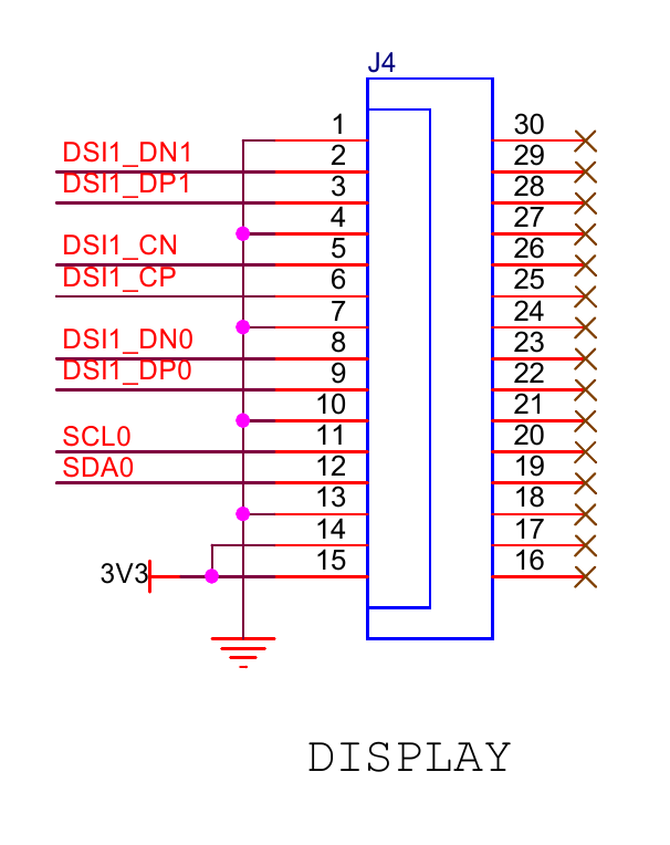
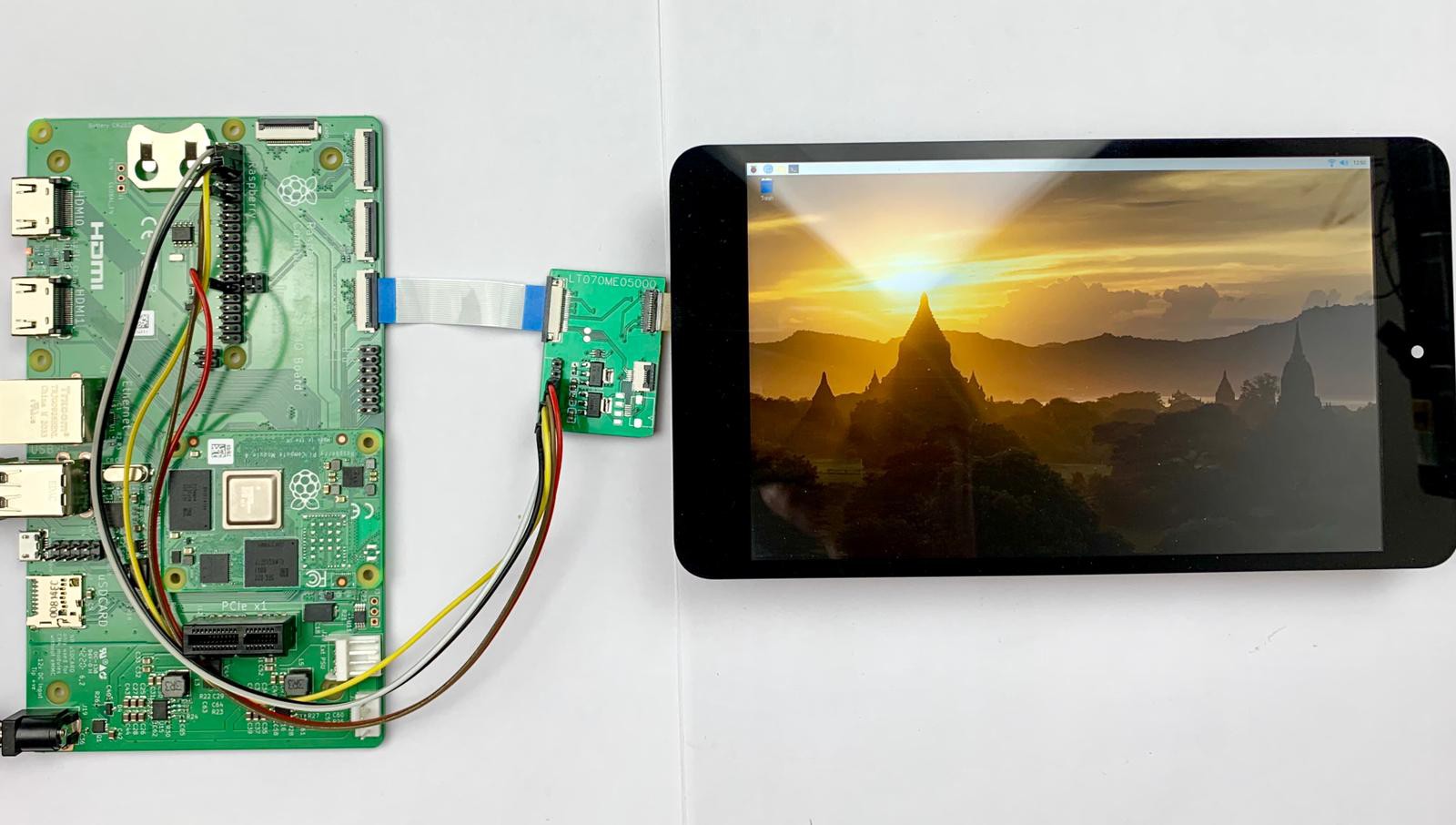
Ideally, you will want a microcontroller or a CPU that has a DSI peripheral, with decent documentation and/or examples on how to use it – that part is important. Linux-capable Raspberry Pi boards can help you here a surprising amount – you may remember the Raspberry Pi DSI header as being proprietary, but that was only true initially. With developments like the official Raspberry Pi screen and open-source graphics drivers aided by that $10k driver bounty they put out, it became viable to connect custom screens. WaveShare DSI screens are a known alternative if you want to get a DSI display for your Pi. On the regular Pi, you only get two lanes of DSI, but that is good enough for many a display. Funnily enough, you can get a third-party display for your Pi that uses the same panel, with two extra chips that seem to run the display without a driver like the official Pi display (this thread on these displays is fascinating!); the display is still limited to the same resolution, the only advantage is a slightly lower price, and the ability to overload your 3.3V rail is a questionable benefit. It’s not quite clear why this display exists, but you might want to resist the temptation.
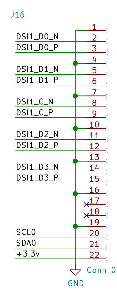
If you’re using a Pi Compute Module, you get entire two DSI peripherals to play with, one four-lane and one two-lane, and it doesn’t take long to find a good few examples of Raspberry Pi Compute Module boards with DSI screens. If you have a Compute Module and its devboard somewhere on a shelf, you can do four-lane DSI, with a Linux-exposed interface that works in the same way alternative OSes do on your phone. Given that CMs are typically used for custom stuff and a hacker using one is more likely to have patience for figuring out DSI panel parameters, a Compute Module baseboard is a pretty popular option to hack on that one cheap DSI display from a tablet that caught your eye! Don’t have a baseboard? You can even etch one, here’s a single-layer breakout with a DSI socket. Not that you don’t need a Compute Module if you’re doing two-lane DSI: a regular Pi will do.
So, get out there and hack – there is a ton of unexplored potential in the never-ending supply of aftermarket screens for older iPhone and Samsung models! Speaking of phones, they are the forefront of DSI hacking, as you might suspect, thanks to all the alternative OS projects and Linux kernel mainlining efforts. You can enjoy fruits of their labour fairly easily, sparing you a logic analyzer foray – reusing a seriously nice DSI display might be as easy as loading a kernel module.
Want A Panel? Linux Is Here To Help
There’s a fun hacker tactic – if you’re looking for an I2C GPIO expander chip, you can scroll through the Linux kernel config file that lists supported GPIO expanders, and find a good few ICs you’ve never known about! What’s great is, you know you’re getting a driver, too.
The same goes for DSI screens, except the payoff is way higher. If you’re on the market for a DSI screen, you can open the list of Linux kernel drivers for various DSI panels. Chances are, all you need is just the physical wireup part, maybe some backlight driving, and a Device Tree snippet.
Want a $20 1920 x 1200 IPS display for your Compute Module? Who doesn’t! Well, wouldn’t you know, the Google Nexus 7 tablet uses one, and the driver for it is in mainline Linux! Just solder together a small FPC-to-bespoke-connector adapter board (or order PCBA), add a Device Tree snippet into your configuration, and off you go; there are even custom boards for using this display with a CM4, it’s that nice.
New displays get added into the kernel all the time; all it takes is someone willing to poke at the original firmware, perhaps load a proprietary kernel module into Ghidra and pull out the initialization sequence, or simply enable the right kind of debug logging in the stock firmware. All of this is thanks to tireless efforts of people trying to make their phones work beyond the bloatware-ridden shackles of the stock Android OS; sometimes, it’s some company doing the right thing and upstreaming a driver for a panel used by hundreds of thousands of devices in the wild.
There are some fun nuances in the display scene, as much as of a “scene” it is – people are just trying to make their devices work for them, then share that work with other people in the same situation, figuring out a display is part of the process. It’s not uncommon that a smartphone will use slightly different screens in the same batch – it’s an uncommon but real issue with alternative OSes like LineageOS, where, say, 10% of your firmware’s users might have their panel malfunction because, despite the phone listing the same model on the lid, their specific phones use a display with a different controller, that only the manufacturer’s firmware properly accounts for.
Our DSI Role Models
These are the basics of what you need to reuse DSI displays as if effortlessly. Now, I’d like to highlight a good few examples of people hacking on DSI, from our coverage and otherwise.
Without a doubt, the first one that springs to mind is [Mike Harrison] aka [mikeselectricstuff], from way back in 2013. I’ve spent a lot of time with the exact iPod Nano being reverse-engineered, and [Mike]’s videos gave me insight into a piece of tech I relied on for a fair bit. For instance, in this video, [Mike] masterfully builds a scoping jig, solders microscoping wires to the tiny PCB, walks us through the entire reverse-engineering process, and successfully reuses the LCD for a project.
Following in [Mike]’s footsteps, we’ve even seen this display reused in an ESP32 project, thanks to a parallel RGB to DSI converter chip!
[Wenting Zhang] reverse-engineering a Macbook Touchbar display is definitely on my favourites list. In this short video, he teaches us DSI fundamentals, and manages to show the entire reverse-engineering process from start to end., no detail spared. Having just checked the video description, the code is open-source, and it’s indeed a RP2040 project – just like I forecasted a good few paragraphs above.
DSI is an interface that is becoming increasingly hacker-friendly – the economies of scale are simply forcing our hand, and even the microcontroller makers are following suit. The official devboard for Espressif’s ESP32-P4, a pretty beefy RISC-V chip, sports a DPI interface alongside the now-usual CSI for cameras. We will see DSI more and more, and I raise a glass of water for numerous hackers soon to reap the fields of DSI. May your harvest be plentiful.
Reminisce.ai is an AI-powered online learning platform that makes it easy and fun to build technology skills and career paths. It uses cheat sheets, quizzes, and games to help you learn IT skills like Kubernetes, React, and AWS. With personalized career coaching, you can develop the right skills for roles like AI Engineer, Blockchain Developer, […]
Today is another board from a friend, [treble], who wants to convert a Yaesu FRG7700 radio to USB-C PD power. It’s yet another review that I’ve done privately, and then realized I’ve made more than enough changes to it, to the point that others could learn from this review quite a bit. With our hacker’s consent, I’m now sharing these things with you all, so that we can improve our boards further and further.
This board’s idea is thought-out and executed well – it replaces a bespoke barrel jack assembly, and is mechanically designed to fit the screw holes and the free space inside the chassis. For USB-PD, it uses a CH32V003 coupled with FUSB302 – I definitely did help pick the latter! For mechanical reasons, this board is split into two parts – one has the USB-C port, whereas the other has the MCU and the PD PHY.
In short, this board is a PD trigger. Unlike the usual PD triggers, however, this one is fully configurable, since it has a 32-bit MCU with good software support, plus, the PD PHY is also well known and easily controllable. So, if you want special behavior like charger-power-dependent profile selection for powering a static resistance load, you can implement it easily – or, say, you can do PPS for variable voltage or even lithium ion battery charging! With a bit of extra code, you could even do EPR (28 V = 140 W power) with this board, instantly making it into a pretty advanced PD trigger, beyond the ones available on the market.
Also, the board has some PCB art, and a very handy filter to get some of the USB-C charger noise out. Let’s take a look at all of these!
Current Flow Improvements
A companion board for this PCB, that hosts the vertical USB-C socket, fitting into the small gap available in the barrel jack space
First of all, the back of the PCB has art. This is a problem. Specifically, the art has to be bigger. See, fabs might struggle drawing thin silkscreen lines. So, I will take the liberty of enlarging it. This board is 25×25 mm in size, after all. Due to the way KiCad works, I’ve had to ask for the original .svg file from [treble] for that. Here’s a tip that I myself should follow more, if you’re adding PCB art, storing its sources alongside the board is pretty valuable for whenever it might need to be regenerated or modified!
This board is seriously nice. It has thick traces for power, and, it makes liberal use of filled zones for higher-current tracks, too! It’s not often that I see these fills used, even for higher-power areas, and truth be told, I get lazy to draw them, but they are possibly the cleanest choice for a board that fulfills a power-related purpose. Also, as usual, it’s just two layers, something dear to my heart.
Now, let’s take a good look at the two layers we have. This is a board that current is supposed to flow through, and if you have an eye for it, you might notice that it will be impeded more than you’d want it to be, in ways that are easy to fix.
Take a look at the board’s bottom layer. It has a ground plane, yes, but there are also tracks going all across it. If you try and visualize the way that ground return current could flow across the board, you might realize that it has to go through a few small slivers of copper; this is despite the ground fill being present on both sides. Let’s fix this.
Here are three spots where you could straightforwardly add ground connectivity purely by moving vias. I usually look out for such spots as part of my after-design cleanup routine – something I might spend a good half an hour on; just, idly glancing at the board in the 3D viewer, looking here and there, trying to notice any things I could improve upon. Here, if you wanted a high return on your investment, you could move these vias and gain whole two new paths for ground return current to flow through.
Moving tracks around will yield way bigger returns for freeing up some ground area. For a start, the SWIO pin, wittily wired up to an SBU pin on the USB-C connector with the trace snaking between the 2.54 mm header pads, doesn’t have to go on B.Cu at all. The VBUS connection of the FUSB302 could also be moved to the left edge, all around the 2.54 mm connector, so that it doesn’t have to cut the ground polygon in half. Furthermore, we could improve upon USB diffpair routing by rotating the CH32V003 90 degrees clockwise, and having the pairs go back onto the front layer again at the top. Part of the 3.3 V track could be routed on the top if you rotate a resistor 180 degrees, and voila, we now have a healthy and plentiful ground polygon.
“Route as much of your board on a single layer as humanly possible” is still a great guideline, and it helps here, too. It also helps if you look at your board and visualize the way that ground return current will flow, from one side to the other, all along the signals.
Only a few small details are left. The ICs don’t have decoupling caps on their 3.3 V inputs, and we could easily add them – cleaner power is always a plus. Oh, and the linear regulator could use a couple more vias from its GND pin – purely for the heat dissipation potential. There’s a 1.5 K resistor used for a USB pull-up, and I2C uses 3.3 K pullups in the same package – I’ve changed them to use 1.5 K too, just as a BOM optimization reminder; should work wonders for I2C.
Implementation Details And Polish
Something I don’t expect hackers to know but is nice to keep in mind – the VBUS pin of the FUSB302 is fault-prone and PSU noise on it can cause the FUSB to die in a way that short-circuits the 3.3 V rail, to the point that the Pinecil soldering iron eventually disconnected it in a new hardware revision, and the community has developed guides to disconnect the VBUS pin. Furthermore, the VBUS connection on the FUSB is not even needed for any part of the PD process; essentially, it’s not even a nice-to-have, all you get is an interrupt that doesn’t carry any meaning in our “bus-powered” arrangement. Let’s disconnect it – that frees up quite a bit of ground and routing space around the FUSB302.
Now, adding a 1:10 resistor divider to an ADC-capable CH32V003 pin would be worthwhile – this lets us measure the voltage we get, checking that it’s indeed the voltage we need. FUSB has provisions to measure voltage on its VBUS pin, but they’re bothersome to use, using an on-MCU ADC is way easier. I’ve also added a 3.6 V Zener diode in 0805 package, clamping the voltage that reaches the GPIO – I don’t expect it to actually be needed, but we do have space for it, and it protects the MCU’s GPIO in case of any assembly errors or voltage spikes; I have previously mis-placed a resistor at a voltage divider, and now I’m worried about others doing it. Worst case, the Zener doesn’t have to be placed at all, and you can just add a capacitor there, smoothing the divided voltage before it reaches the ADC.
What else? Here’s something to consider – the radio might not be happy with 5 volts on its power input, which is an inevitability given how the USB-C negotiation process works. Remember, first, you get 5 V, and then you have to negotiate further up. This is why PD trigger ICs tend have a PG pin, that you can connect to a P-FET gate, and that pin is only driven after a successful negotiation. In our case, we have MCU GPIOs we can use instead!
CH32V003 pinout diagram courtesy of [Tengo10]’s pinout generator scriptFor that to work, let’s rewire the VBUS on this board. The MCU and its 3.3 V linear regulator can be powered from the raw USB-C input, we won’t gate them with the FET, of course, that’d lead to a chicken and egg problem. It makes sense to power the Pi filter through the FET, though – mostly because we have some board space between the USB-C input and the Pi filter, where a SOT-23 FET could very nicely fit. The radio could consume as much as 3 A at 12 V; at least, that’d be the maximum capability of a typical USB-C PSU you could use with this board. My FET of choice, then, is AO3401 – a classic FET that works at 30 V 4 A, and will even let this board be a pretty generic trigger board if needed, and; higher current, you can stack one more SOT23 FET on top.
With an NPN driver and a provisional 3:1 divider for the gate voltage, the “power good” circuit fits into the board space wonderfully. If it’s not needed, it can be easily jumpered with a 0 R resistor across the FET pads, but adding this circuit retrospectively would be bothersome – it helps that we have the footprints for it. Remember, traces and footprints are free to add, fundamentally – just like silkscreen markings.
How Will You Use Your Board?
Another great thing to visualize is – after you assemble your board, how will you interact with it? Here, [treble] still has to write the USB-PD firmware – in C++, no less, my MicroPython stack won’t be directly applicable, as much as I will help, but [Ralim]’s open-source PD stack used in the Pinecil could work wonderfully! While integrating that, she will have to debug things. Possibly, might even have to debug it some more later on, with the board installed into the radio chassis. It’s a project one hacker could pull off without a doubt, and, there’s things you could add to your board that will help.
The SWIO pin of the CH32V003 goes to an SBU pin on the USB-C socket. This is a great decision, because you can easily reflash the MCU without disassembling the entire radio – just have a USB-C plug with SBU exposed and that’s enough. Also, when I’m thinking about it, it might be troublesome during active development, because [treble] will have to constantly unplug and plug the PSU and the programming plug while debugging the in-progress firmware. Now, she could solder to the 2.54 mm pin headers, sure – alternatively, you could add an extra SWIO header at the edge and make her job a bit easier. I can’t find much space for it, sadly, so I suppose a female header with longer male pins (Arduino and Wemos shield style) can do just as well, also allowing to probe CC pins as a bonus.
I feel like there’s a good few more things you can add to improve development and usage comfort. Will there be a failure mode where the board has to signal to the user that something’s gone wrong – say, with a 5 V USB-C PSU inserted? Let’s add two LEDs on one pin – could even do WS2812 sometime later. What about I2C communications, what if tapping them would be useful during the board’s development? Let’s add a QWIIC socket and pull the I2C lines onto it – not for expansions, but rather, so that you have a socket you can easily wire up to a logic analyzer, plug it in and unplug it at any point.
There’s some arguments to be made for breaking out as many CH32V003 pins as possible. I will refrain from it, as much as it’s tempting – at this point, there isn’t a lot of board space in the spots where it matters. It would be cool to have them on testpoints though! Speaking about that, I’ve just realized – you could add a tiny SMD three-position DIP switch onto the back of the board reasonably easily, so that you can have “profiles” for the trigger board, CH224 PD trigger board style. I’ve found the tiniest three-position SMD DIP switch that LCSC has, then added it to the back of the board, trying to still have the ground fill as intact as possible – the idea is that this is a nice feature for whenever the board might be used as a more general-purpose trigger board. When not populated, it serves as a breakout for three ADC-capable GPIOs, GND, and 3.3 V!
Now, I’d like to emphasize: the DIP switch is not exactly necessary in this project. It falls into “something that’d be cool to fit in space left over, if the board is to be used in an entirely different setting”. Overall, I try not to push features this remote onto people while doing design review – plus, it does clash with the silkscreen. So, this addition is easily removable from the PCB files, and it doesn’t have to be populated either. Also, I’ll stop the additions here, to avoid feature creep.
That about wraps it up for things I feel like this board needs. Let’s talk about an aspect where I’d like your opinion.
Questions For The Audience
Now, here’s a question for the audience, on two things I’m not well-versed on. First one is – here’s a Pi filter. The purpose is filtering out 300 KHz USB-C charger switching frequency that [treble] has noticed being produced by a USB-C charger she’s picked. Having simulated this filter in LTSpice, it appears to be good for filtering out 200 KHz and above. Does that look correct? And, any things she should look out for when it comes to component choices?
Another question is – the ground cutout under the Pi filter. My understanding is – the more ground, all over the board, the better. [treble] decided to remove ground under the Pi filter, as far as I recall, due to a gut feeling that it’d decrease noise imposed by the inductor. Does that make sense? I’m tempted to say “no”, but I can’t formulate a good enough explanation on the specific downsides and how it might need, which is why I’m asking you.
Another board reviewed, and due to the way it’s built, I can easily imagine ordering a dozen for use in my own projects – thanks to [treble] for sharing this, and I hope this feedback helps! As usual, if you would like a design review for your board, submit a tip to us with [design review] in the title, linking to your board files. KiCad design files strongly preferred, both repository-stored files (GitHub/GitLab/etc) and shady Google Drive/Dropbox/etc .zip links are accepted.
I thank [Julianna] for helping me check the the CH32V003 circuit!
Most of the Hackaday community would never wire a power supply to a circuit without knowing the expected voltage and the required current. But our mechanical design is often more bodged. We meet folks who carefully budget power to their microcontroller, sensors, and so on, but never measure the forces involved in their mechanical designs. Then they’re surprised when the motor they chose isn’t big enough for the weight of their robot.
An obstacle to being more numbers oriented is lack of basic data about the system. So, here are some simple tools for measuring dynamic properties of small mechanisms; distances, forces, velocities, accelerations, torques, and other things you haven’t thought about since college physics. If you don’t have these in your toolkit, how do you measure?
Distance
For longer distances the usual homeowner’s tools work fine. The mechatronics tinkerer benefits from two tools on the small end. A dial or electronic caliper for measuring small things, and a thickness gauge (or leaf gauge) for measuring small slots.
A thickness gauge is just metal leaves in different thicknesses, bolted together at one end. Find a combination of leaves that just fits in the space.
Force
Here’s four force measuring tools we use to cover different magnitudes of force: a postage scale, a push stick, a spring scale, and a letter scale. The postage scale is best purchased. For big things, the bathroom scale works.
A push stick is a force measurement device that you can make yourself. We first saw one of these used to tune slot cars, but they’re universally useful. It’s a simple pen shaped device made with a barrel from any small transparent parts tube, a spring, and a plunger with a protruding pin. Grasp the barrel and push the gizmo with the pin, and you can read the force off the tube.
If you need it to be calibrated, remember that you just bought a postage scale. Push it into the scale and mark off reasonable increments. Make several, in different sizes. A Z or L shaped plunger is useful for hard to reach places.
The conventional spring tension scale is useful, but most commercial ones are terribly made and inaccurate. You can make yourself a better one. They are useful for measuring the spring constant of springs, for learning the tractive effort needed to move a robot, finding the center of gravity of a robot arm, and a hundred other ‘how much oomph’ things. Again, it’s just a matter of connecting a hook to a spring, and measuring its deflection.
For yet lighter weights, you could buy a letter scale, at least in the old days. Today you might have to make your own. It can be as simple as a piece of spring steel fixed to a sheet of calibrated cardboard.
Torque
Torque measurements are good not only for sizing actuators, but for measuring efficiency.
How you do torque measurements depend on the speed you want to make them at. For static loads, just put a lever of known length on the shaft and measure the force. Torque = distance * force. For fast rotating systems, you can run the system at a known speed and measure the electrical energy used.
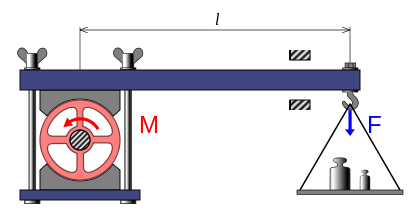
Schematic of a Prony brake by [MatthiasDD]If you just want to apply a varying known torque to measure efficiency, your life is much easier. Mount a broad wheel of some sort on the shaft — RC airplane tires work well. Drape a piece of ribbon over the tire. Anchor it at the “out” end and hang a small weight at the “in” end. This is a Prony Brake, and it’s a useful device to know about. The force on the outside of the wheel is just enough to lift the weight – after that the ribbon slips. The measured torque is then the weight times the wheel radius.
You may also want to measure speeds and accelerations. Here, the ubiquity of cell phone cameras is your friend. Suppose you’re animating a crane on your model railroad. Record yourself on video moving the crane with your hands against a protractor to get a feel for speed and acceleration. In video editing software check the positions for various frames, and you now have position changes. The number of frames and distance can help you calculate the speed, and the change in speed vs time is acceleration.
If your mechanism is moving too fast for video, use a fast phototransistor or hall effect device and an oscilloscope, or gear down by holding a toy wheel against the shaft and measure the more slowly rotating wheel.
In the crane example, the torque you need to supply is the frictional torque plus the acceleration torque, and to calculate the acceleration torque you need the moment of inertia. For refresher: angular acceleration = torque / moment of inertia (ω = τ / I) and moment of inertia = mass * radius2 (I = m * r2 ) for point mass.
You can drive the crane with a repeatable torque, say using a pulley and weight or a motor, and get the acceleration ω1 from the still frames on your video. If you repeat this with a known mass m a known distance r from the shaft axis, like a lump of putty on the end of the crane arm, you can get a second value: ω2.
Write the ω = τ / I equations, ω1 = τ / Icrane and ω2 = τ / (Icrane + r 2 * m). Combining and isolating Icrane and holding our tongues just right, Icrane = r2 * m / (ω1 / ω2 – 1).
Be careful to subtract the moment of inertia of your measuring apparatus, and add in the moment of inertia of the final drive if needed. Now you can size your servo with some confidence. Believe me, once you’ve done this a couple times, you’ll never go back to winging it.
Power
The easiest way to get a ballpark feel for power is to simply measure the system’s consumed power by measuring the electrical power at the motor, but this ignores losses in the drive train. And losses are one of the really interesting things to measure. Bad performance is usually friction, and efficiency is a goal for other reasons than just motor sizing or battery life. It’s a measure of how janky your setup is.
Does your model train or robot run poorly? Set it to climb a steep grade on a test track. Calculate the work it does: mass * height change. Measure the input electrical power and the time, Energy = V*I*T. You now have an idea of how much the actual power consumption differs from the maximally efficient system. Any power that went in but didn’t appear as potential energy in the choo-choo’s new position is frictional loss. Now you can experiment with loosening and tightening screws, changing gear mesh, and such, and have some idea if you’re making things better or worse.
Conclusion
None of the above was rocket science, and you don’t need to do some complex FEM analysis to make the average hacker project. But a bit of real engineering can go a long way towards more reliable mechanisms, and that starts with knowing the numbers you’re dealing with. Taking the required measurements can be simple if you know how to build the tools you need, and your life will be easier with some numbers to guide you.
Who doesn’t want to use a programming language that is designed to be reliable, straightforward to learn and also happens to be certified for everything from avionics to rockets and ICBMs? Despite Ada’s strong roots and impressive legacy, it has the reputation among the average hobbyist of being ‘complicated’ and ‘obscure’, yet this couldn’t be further from the truth, as previously explained. In fact, anyone who has some or even no programming experience can learn Ada, as the very premise of Ada is that it removes complexity and ambiguity from programming.
In this first part of a series, we will be looking at getting up and running with a basic desktop development environment on Windows and Linux, and run through some Ada code that gets one familiarized with the syntax and basic principles of the Ada syntax. As for the used Ada version, we will be targeting Ada 2012, as the newer Ada 2022 standard was only just approved in 2023 and doesn’t change anything significant for our purposes.
Toolchain Things
The go-to Ada toolchain for those who aren’t into shelling out big amounts of money for proprietary, certified and very expensive Ada toolchains is GNAT, which at one point in time stood for the GNU NYU Ada Translator. This was the result of the United States Air Force awarding the New York University (NYU) a contract in 1992 for a free Ada compiler. The result of this was the GNAT toolchain, which per the stipulations in the contract would be licensed under the GNU GPL and its copyright assigned to the Free Software Foundation. The commercially supported (by AdaCore) version of GNAT is called GNAT Pro.
Obtaining a copy of GNAT is very easy if you’re on a common Linux distro, with the package gnat for Debian-based distros and gcc-ada if you’re Arch-based. For Windows you can either download the AdaCore GNAT Community Edition, or if you use MSYS2, you can use its package manager to install the mingw-w64-ucrt-x86_64-gcc-adapackage for e.g. the new ucrt64 environment. My personal preference on Windows is the MSYS2 method, as this also provides a Unix-style shell and tools, making cross-platform development that much easier. This is also the environment that will be assumed throughout the article.
Hello Ada
The most important part of any application is its entry point, as this determines where the execution starts. Most languages have some kind of fixed name for this, such as main, but in Ada you are free to name the entry point whatever you want, e.g.:
with Ada.Text_IO;
procedure Greet is
begin
    -- Print "Hello, World!" to the screen
    Ada.Text_IO.Put_Line ("Hello, World!");
end Greet;
Here the entry point is the Greet procedure, because it’s the only procedure or function in the code. The difference between a procedure and a function is that only the latter returns a value, while the former returns nothing (similar to void in C and C++). Comments start with two dashes, and packages are imported using the with statement. In this case we want the Ada.Text_IO package, as it contains the standard output routines like Put_Line. Note that since Ada is case-insensitive, we can type all of those names in lower-case as well.
Also noticeable might be the avoidance of any symbols where an English word can be used, such as the use of is, begin and end rather than curly brackets. When closing a block with end, this is post-fixed with the name of the function or procedure, or the control structure that’s being closed (e.g. an if/else block or loop). This will be expanded upon later in the series. Finally, much like in C and C++ lines end with a semicolon.
For a reference of the syntax and much more, AdaCore has an online reference as well as a number of freely downloadable books, which include a comparison with Java and C++. The Ada Language Reference Manual (LRM) is also freely available.
Compile And Run
To compile the simple sample code above, we need to get it into a source file, which we’ll call greet.adb. The standard extensions with the GNAT toolchain are .adb for the implementation (body) and .ads for the specification (somewhat like a C++ header file). It’s good practice to use the same file name as the main package or entry point name (unit name) for the file name. It will work if not matched, but you will get a warning depending on the toolchain configuration.
Unlike in C and C++, Ada code isn’t just compiled and linked, but also has an intermediate binding step, because the toolchain fully determines the packages, dependencies, and other elements within the project before assembling the compiled code into a binary.
An important factor here is also that Ada does not work with a preprocessor, and specification files aren’t copied into the file which references them with a with statement, but only takes note of the dependency during compilation. A nice benefit of this is that include guards are not necessary, and headaches with linking such as link order of objects and libraries are virtually eliminated. This does however come at the cost of dealing with the binder.
Although GNAT comes with individual tools for each of these steps, the gnatmake tool allows the developer to handle all of these steps in one go. Although some prefer to use the AdaCore-developed gprbuild, we will not be using this as it adds complexity that is rarely helpful. To use gnatmate to compile the example code, we use a Makefile which produces the following output:
Although we just called gnatmake, the compilation, binding and linking steps were all executed subsequently, resulting in our extremely sophisticated Hello World application.
For reference, the Makefile used with the example is the following:
Great, so now you have a working development environment for Ada with which you can build and run any code that you write. Naturally, the topic of code editors and IDEs is one can of flamewar that I won’t be cracking open here. As mentioned in my 2019 article, you can use AdaCore’s GNAT Programming Studio (GPS) for an integrated development environment experience, if that is your jam.
My own development environment is a loose constellation of Notepad++ on Windows, and Vim on Windows and elsewhere, with Bash and similar shells the environment for running the Ada toolchain in. If there is enough interest I’d be more than happy to take a look at other development environments as well in upcoming articles, so feel free to sound off in the comments.
For the next article I’ll be taking a more in-depth look at what it takes to write an Ada application that actually does something useful, using the preparatory steps of this article.
PuzzleGenerator.ai is an innovative tool harnessing the power of AI to transform the world of custom puzzles. It creates unique puzzle designs tailored to your individual preferences, delivering a personalized experience. You can view the latest and featured puzzles that were created using the tool on the home page. Alternatively, you can sign in to […]