The modern hacker and maker has a truly incredible arsenal of tools at their disposal. High-tech tools like 3D printers, laser cutters, and CNC routers have all become commonplace, and combined with old standbys like the drill press and mini lathe, it sometimes seems like we’ve finally peaked in terms of what the individual is realistically capable of producing in their own home. But occasionally a new tool comes along, and it makes us realize that there are still avenues unexplored for the home gamer.
 After spending the last few weeks playing with it, I can confidently say the eufyMake E1 UV printer is one of those tools. The elevator pitch is simple: with a UV printer, you can print anything on anything. As you can imagine, the reality is somewhat more complex, but the fact that you can toss a three dimensional object in the chamber and spray it with a high-resolution color image with a few button presses holds incredible creative potential. Enough that the Kickstarter for the $1,700 printer has already raised a mind-boggling $27 million at the time of this writing, with more than a month yet to go before crossing the finish line.
If you’re on the fence about backing the campaign, or just have doubts about whether or not the machine can do what eufyMake claims, I’ll put those concerns to rest right now — it’s the real deal. Even after using the machine for as long as I have, each time a print job ends, I find myself momentary taken aback by just how good the end result is. The technology inside this machine that not only makes these results possible, but makes them so easily obtainable, is truly revolutionary.
That being said, it’s not a perfect machine by any stretch of the imagination. While I never ran into an outright failure while using the eufyMake E1, there’s a fairly long list of issues which I’d like to see addressed. Some of them are simple tweaks which may well get sorted out before the product starts shipping this summer, while others are fundamental to the way the machine operates and could represent an opportunity for competitors.
Theory of Operation
Before we go any further, I think it’s important to explain how the eufyMake E1 works. Not only because UV printers aren’t the kind of thing that most of us have had first-hand experience with, but because I want readers to understand how much the product gets right.
In the most basic case, you’ll open up the door of the E1, and stick an object on the bed. (There’s a larger bed that you can swap in for over-sized objects, but you have to run the printer with the doors open.) That’s a literal “stick”, by the way, as the bed is designed to be tacky to provide a bit of hold on smaller objects which might otherwise jump around as the machine moves. The E1 will then go through an automated process that includes flashing lights and sweeping red laser beams. This provides the machine with a 3D scan of the object on the bed, which is necessary for positioning the print head later on.
At this point, the software (available for Windows, Mac, and mobile devices) will present the user with a “bird’s eye view” of the bed and any objects on it. From here you can either use the basic art tools in the software, or more likely, import some artwork created in a more comprehensive piece of software. In either event, the process is the same, in that you virtually apply your artwork directly on the overhead image. Once you’re happy with how it looks, you hit “Print”, pick a few options relating to the target’s surface material and the print quality, and off it goes.
Printing is admittedly slower than I had expected. Depending on the image complexity, even a palm-sized job could take 20 or 30 minutes. While I never pushed it so far personally, I’ve heard from other testers that larger projects can take hours to complete. In that way, it’s a lot like a 3D printer — you aren’t the one that has to do all that work, so who cares if the process takes an hour or two, just let it run and come back to it later. In my experience, the results have always been more than worth the wait.
Practical Examples
I’ve said as much previously, but we don’t take reviews and hands-on articles like this lightly here at Hackaday. Companies offer to send us hardware on an almost daily basis, but we turn down the vast majority of them as we just don’t think they’re a great fit for our audience. Is the average Hackaday reader really going to be interested in a review of yet another 3D printer or laser engraver? Probably not.
So before we agreed to take a look at the eufyMake E1, Elliot and I talked a bit about how such a machine would be used in our community specifically. We came up with a few things we thought hardware hackers would want to do with this kind of capability, and I made sure to focus on those applications over the more “crafty” demonstrations that you may have seen elsewhere.
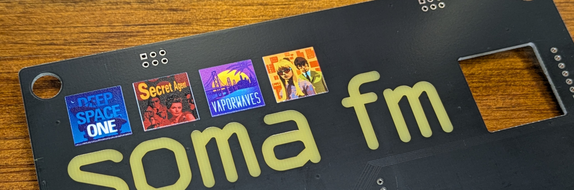
Full-Color PCB Art
While we’re starting to see board fabs support color silkscreens, it’s not a capability that’s necessarily ready for prime time. Beyond the mixed results we’ve heard from those in the community in terms of the quality of the resulting boards, there’s some unfortunate software/vendor lock-in that we’d just as soon avoid. So what if you could skip all that and simply put your professionally made PCBs in the E1 and have it apply your artwork to them?
In this fairly simple example I’ve taken one of the spare boards from my Soma FM badge and applied a few high resolution images onto it. I never really had any doubt that the eufyMake E1 could do PCB art, but still, it was extremely satisfying to see it in person.
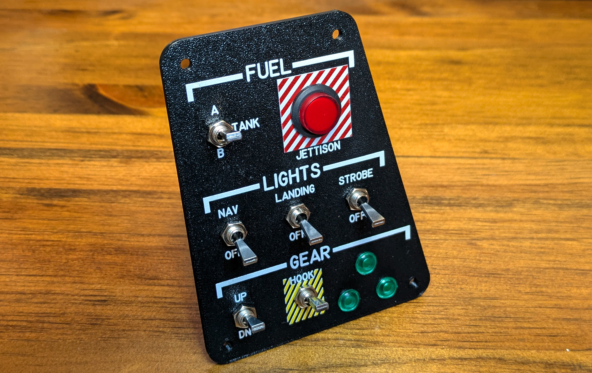
Control Panels
High quality control panels have always been tricky to produce at home. Sure there’s ways to pull it off, such as the recent trick we covered that used specially treated inkjet printouts, but they tend to be time consuming and the results are highly dependent on the material you’re working working. With the UV printer, front panels are a breeze and you’ll get consistent results whether you’re working with plastic or metal.
For this example I came up with a flight-sim style panel inspired by various fighter jets. The workflow was actually quite nice: I designed the panel itself in OpenSCAD, and then exported it as both a 3D STL and 2D DXF file. The 3D file got printed out, and the 2D file was imported into Inkscape. With a 1:1 outline of the panel in Inkscape, I could position the text and images knowing they would line up perfectly with the real-world object. I exported my Inkscape design as an SVG, loaded it into the E1’s software, and applied it to the printed panel.
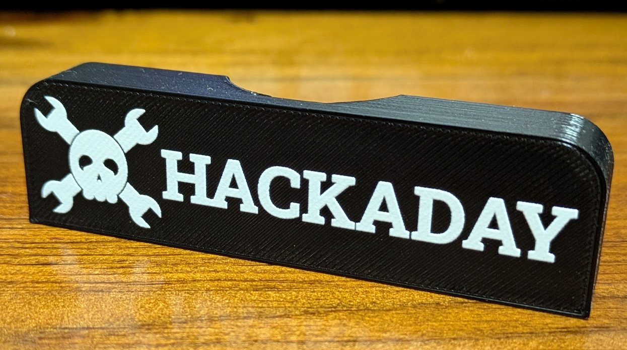
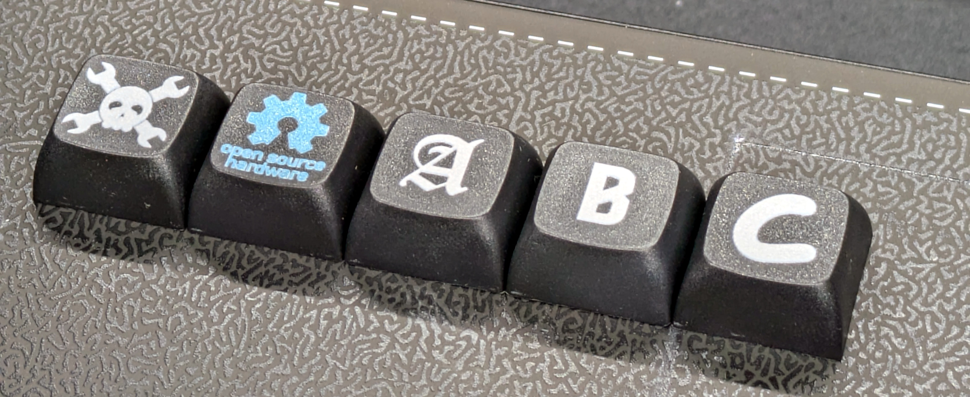
Truly Custom Keycaps
We’ve seen incredible interest in bespoke keyboards over the last few years, and customized keycaps are a big part of that. But even the most decked out keyboards are generally still using off-the-shelf keycaps. But why settle for that when you can buy blank caps and apply whatever text or artwork you wish on them?
These are such a perfect application for the E1 that I imagine it’s going to ignite something of a custom keycap revolution once the printer gets into consumer’s hands. Whether you want each key to be the face of a different anime character, or want all the legends to be in Comic Sans, you have complete control. They also serve as a great example of the fine detail work that’s possible on the machine.
The Perfect PCB Machine?
I know what you’re thinking: “Stop teasing me, can the damn thing make PCBs or not!” The short answer is yes…but the long answer is worth a bit more examination.
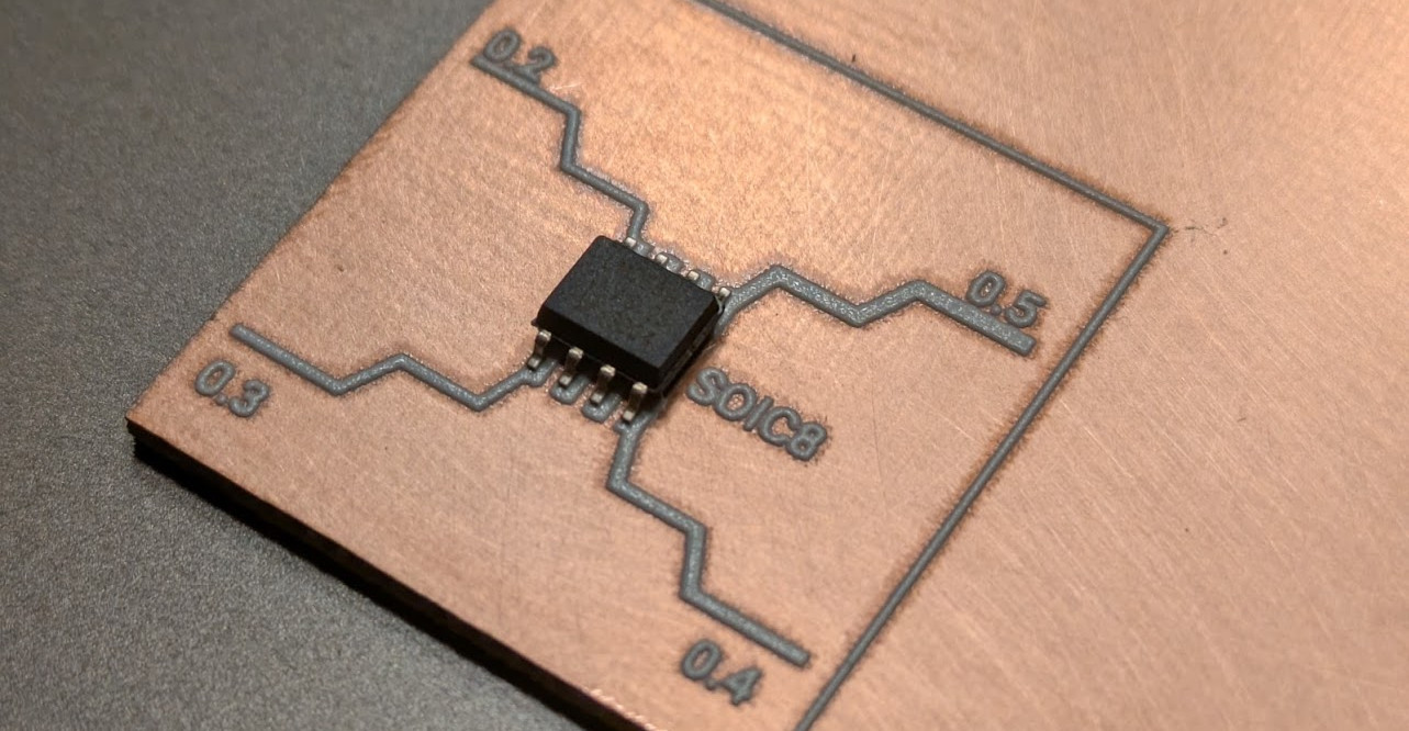
The UV print seems to work very well as an etch resist, as it was completely unfazed by its encounter with ferric chloride. In fact, the first challenge was figuring out how to get the stuff off after etching. Alcohol, turpentine, and paint thinner did nothing to it. Eventually I found that soaking the board in acetone will break down the bond between the printed layer and the copper — you still need to peel it off, but once you get under an edge with a razor blade it parts without too much trouble.
Early results look promising. The lines aren’t as clean as I’d like, so it will probably have problems with tight pitch parts, but the traces were intact down to 0.2 mm, and the pads for the SOIC8 footprint I picked as a test were properly isolated from each other. At this point, it’s a working PCB that’s at least as good as something made with the old school toner transfer method. But the E1 promises so much more.
Putting the board back in the machine, I was able to spray it with additional layers that act as both a soldermask and silkscreen. While I want to experiment a bit more and refine the techniques involved, even this first attempt produced a remarkably professional looking board with very little manual effort on the user’s part.
That said, while this proof of concept shows it’s clearly possible to produce impressive boards on the machine, the process is made frustrating by various limitations of the hardware and software.
One-Off Versus Production
Let’s be clear, as a product, the eufyMake E1 is designed to let crafty folks put pictures of their kids on slate coasters and emblazon mugs with the logo of their favorite sports team. The software and hardware is clearly designed to make it as easy as possible to toss an object into the printer, get your image virtually aligned on it, and then spray it on. At this, the product excels, and I have no doubt it will be a commercial success.
But while hardware hackers are certainly not immune to the charms of putting memes and logos on their possessions, we also have slightly higher demands. If we’re talking about using it for producing PCBs, or even just adding art to existing boards, we’re looking for high positional accuracy and repeatability.
To that end, I have to report that the E1 is not particularly well suited to such technical tasks. It can be pushed into service, but there’s several aspects of the product that would really need to be addressed before this could be a workhorse for the hackerspace.
Lack of Physical Indexing
As it stands, the bed on the eufyMake E1 is a completely flat surface, with no provisions for work holding or indexing. You’re expected to visually align your print each time — workable for one or two copies of an object, but excruciating beyond that.
Now you might be thinking that this is an easy enough problem to remedy…but you’re probably forgetting that 3D bed scan. Any fixture you come up with to hold your object in position runs the risk of screwing up the scan and causing the print to abort. Even trying to tape a PCB down with blue painter’s tape would occasionally trigger an error during the scan as the machine couldn’t find a clearly defined edge.
As you’ll see below, I’ve had some success with very thin 3D printed fixtures that avoid the ire of the scanner. Long term, I’d like to see an alternate bed that resembled a CNC fixture plate, so that multiple parts can be held in position with low-profile pegs.
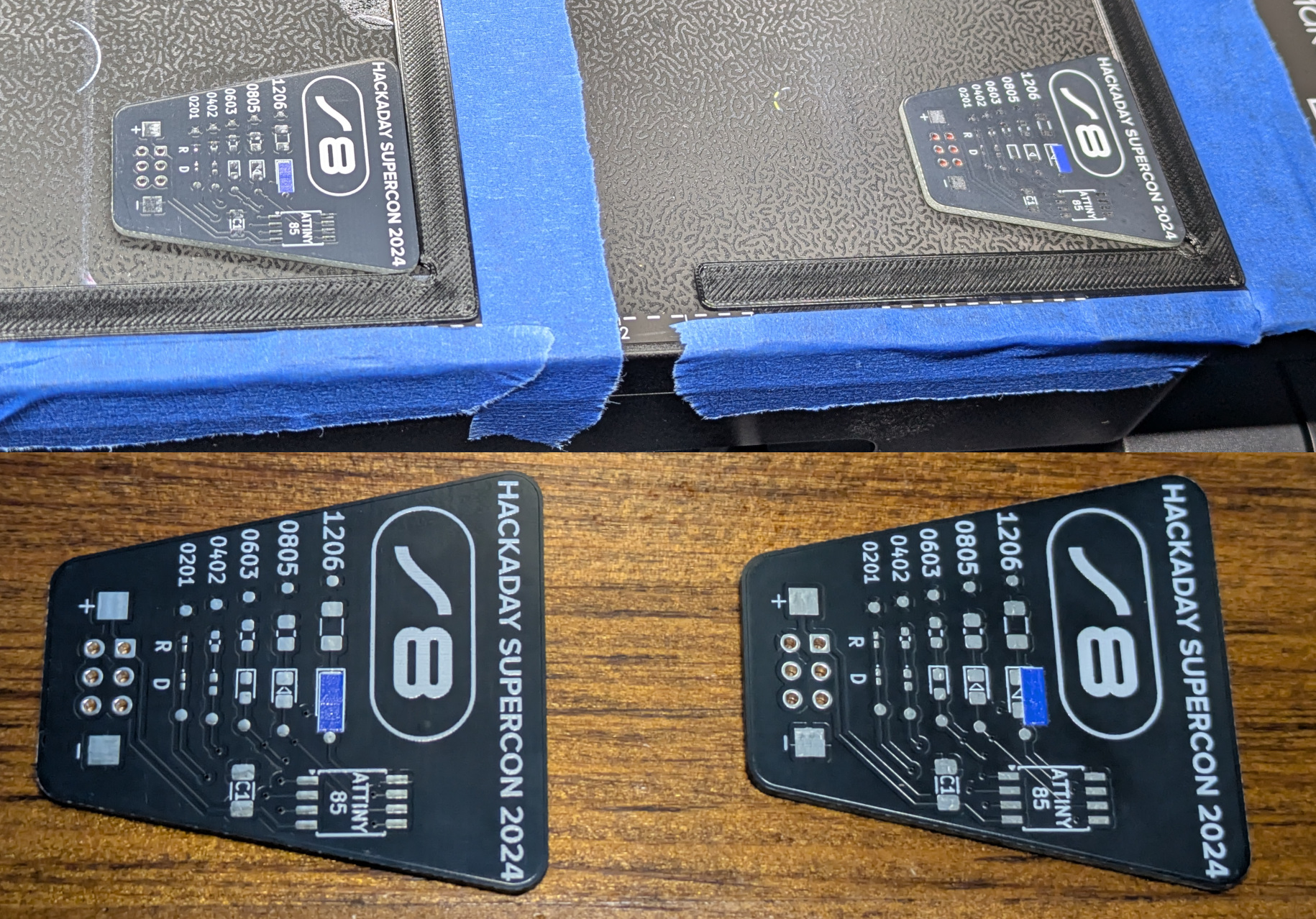
The Parallax View
At the suggestion of Thomas Flummer, I printed out a few thin (1.2 mm) jigs that could be taped down to the bed and help position multiple objects for batch processing. This is much better than having to eyeball things each time, but it uncovered a new issue.
For objects in the center of the bed, the optical alignment system works pretty well. It should get you within a millimeter or so on the first attempt, but it’s way off on the edges of the bed. Take a look at the following example: the in the software, both blue rectangles were perfectly aligned within the footprint of the 1206 LED:
As you can see the alignment on the board in the center is pretty locked in, but on the other board, it’s halfway out of the footprint. This might be close enough if you’re making grandma some Christmas ornaments, but it won’t cut it for SMD work.
The good news is that you can go back into the software and move objects at the sub-millimeter level by typing in the desired coordinates. This will cause the visual representation to become misaligned, but so long as you know where the target is in the real-world, it doesn’t matter. So if you can afford a bit of trial-and-error, it’s possible to get the alignment dialed in even across multiple objects on the bed.
The Shape of Things to Come?
As I said at the start, the eufyMake E1 is not a perfect machine. Beyond the major issues I’ve outlined here, there’s all sorts of weird quirks and limitations I’ve run into during my time with it. For example, why don’t the lights inside the enclosure turn on when the door is open? Why doesn’t the printer itself have a small screen to display status information? We won’t even get into the fact that all your interactions with the printer have to go through the cloud — there isn’t even so much as a USB port on the printer to allow local control.
But at the end of the day, I’m still extremely excited about this machine. The fact is, there’s really nothing else quite like it on the market, at least, not at this price anyway. It reminds me a bit of the MakerBot Cupcake 3D printer, or even the K40 laser. It represents such a huge leap forward in capability for the individual that it’s easy to excuse the rough edges.
Like those machines, I believe the eufyMake E1 will set many of the standards for the products that come after it. You may never own this particular UV printer, but I’m willing to bet that after a few hardware generations, when the cost of the technology is driven even lower thanks to increased competition, the printer that you do buy will be able to trace its lineage back to this moment.