Electrostatic droplet capture system installed on an HVAC condenser. (Credit: Infinite Cooling)
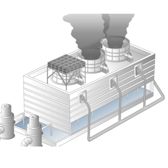
As a common feature with thermal power plants, cooling towers enable major water savings compared to straight through cooling methods. Even so, the big clouds of water vapor above them are a clear indication of how much cooling water is still effectively lost, with water vapor also having a negative impact on the environment. Using so-called plume abatement the amount of water vapor making it into the environment can be reduced, with recently a trial taking place at a French nuclear power plant.
This trial featured electrostatic droplet capture by US-based Infinite Cooling, which markets it as able to be retrofitted to existing cooling towers and similar systems, including the condensers of office HVAC systems. The basic principle as the name suggests involves capturing the droplets that form as the heated, saturated air leaves the cooling tower, in this case with an electrostatic charge. The captured droplets are then led to a reservoir from which it can be reused in the cooling system. This reduces both the visible plume and the amount of cooling water used.
In a 2021 review article by [Shuo Li] and [M.R. Flynn] in Environmental Fluid Mechanics the different approaches to plume abatement are looked at. Traditional plume abatement designs use parallel streams of air, with the goal being to have condensation commence as early as possible rather than after having been exhausted into the surrounding air. Some methods used a mesh cover to provide a surface to condense on, while a commercially available technology are condensing modules which use counterflow in an air-to-air heat exchanger.
Other commercial solutions include low-profile, forced-draft hybrid cooling towers, yet it seems that electrostatic droplet capture is a rather new addition here. With even purely passive systems already seeing ~10% recapturing of lost cooling water, these active methods may just be the ticket to significantly reduce cooling water needs without being forced to look at (expensive) dry cooling methods.
Top image: The French Chinon nuclear power plant with its low-profile, forced-draft cooling towers. (Credit: EDF/Marc Mourceau)
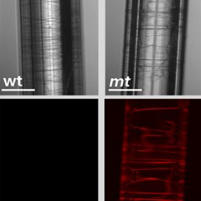
Regular vs gene-edited spider silk with a fluorescent gene added. (Credit: Santiago-Rivera et al. 2025, Angewandte Chemie)
Continuing the scientific theme of adding fluorescent proteins to everything that moves, this time spiders found themselves at the pointy end of the CRISPR-Cas9 injection needle. In a study by researchers at the University of Bayreuth, common house spiders (Parasteatoda tepidariorum) had a gene inserted for a red fluorescent protein in addition to having an existing gene for eye development disabled. This was the first time that spiders have been subjected to this kind of gene-editing study, mostly due to how fiddly they are to handle as well as their genome duplication characteristics.
In the research paper in Angewandte Chemie the methods and results are detailed, with the knock-out approach of the sine oculis (C1) gene being tried first as a proof of concept. The CRISPR solution was injected into the ovaries of female spiders, whose offspring then carried the mutation. With clear deficiencies in eye development observable in this offspring, the researchers moved on to adding the red fluorescent protein gene with another CRISPR solution, which targets the major ampullate gland where the silk is produced.
Ultimately, this research serves to demonstrate that it is possible to not only study spiders in more depth these days using tools like CRISPR-Cas9, but also that it is possible to customize and study spider silk production.
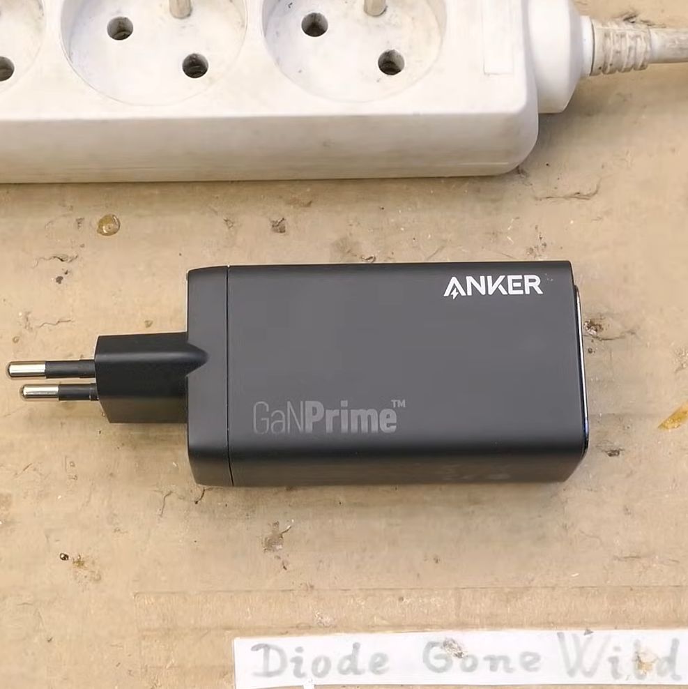
Taking a break from his usual prodding at suspicious AliExpress USB chargers, [DiodeGoneWild] recently had a gander at what used to be a good USB charger.
The Anker 737 USB charger prior to its autopsy.
Before it went completely dead, the Anker 737 GaNPrime USB charger which a viewer sent him was capable of up to 120 Watts combined across its two USB-C and one USB-A outputs. Naturally the charger’s enclosure couldn’t be opened non-destructively, and it turned out to have (soft) potting compound filling up the voids, making it a treat to diagnose. Suffice it to say that these devices are not designed to be repaired.
With it being an autopsy, the unit got broken down into the individual PCBs, with a short detected that eventually got traced down to an IC marked ‘SW3536’, which is one of the ICs that communicates with the connected USB device to negotiate the voltage. With the one IC having shorted, it appears that it rendered the entire charger into an expensive paperweight.
Since the charger was already in pieces, the rest of the circuit and its ICs were also analyzed. Here the gallium nitride (GaN) part was found in the Navitas GaNFast NV6136A FET with integrated gate driver, along with an Infineon CoolGaN IGI60F1414A1L integrated power stage. Unfortunately all of the cool technology was rendered useless by one component developing a short, even if it made for a fascinating look inside one of these very chonky USB chargers.
Although the idea of containing a plasma within a magnetic field seems straightforward at first, plasmas are highly dynamic systems that will happily escape magnetic confinement if given half a chance. This poses a major problem in nuclear fusion reactors and similar, where escaping particles like alpha (helium) particles from the magnetic containment will erode the reactor wall, among other issues. For stellarators in particular the plasma dynamics are calculated as precisely as possible so that the magnetic field works with rather than against the plasma motion, with so far pretty good results.
Now researchers at the University of Texas reckon that they can improve on these plasma system calculations with a new, more precise and efficient method. Their suggested non-perturbative guiding center model is published in (paywalled) Physical Review Letters, with a preprint available on Arxiv.
The current perturbative guiding center model admittedly works well enough that even the article authors admit to e.g. Wendelstein 7-X being within a few % of being perfectly optimized. While we wouldn’t dare to take a poke at what exactly this ‘data-driven symmetry theory’ approach exactly does differently, it suggests the use machine-learning based on simulation data, which then presumably does a better job at describing the movement of alpha particles through the magnetic field than traditional simulations.
Top image: Interior of the Wendelstein 7-X stellarator during maintenance.
Fabrication of uranium-based components via DLP. (Zanini et al., Advanced Functional Materials, 2024)
Within the nuclear sciences, including fuel production and nuclear medicine (radiopharmaceuticals), often specific isotopes have to be produced as efficiently as possible, or allow for the formation of (gaseous) fission products and improved cooling without compromising the fuel. Here having the target material possess an optimized 3D shape to increase surface area and safely expel gases during nuclear fission can be hugely beneficial, but producing these shapes in an efficient way is complicated. Here using photopolymer-based stereolithography (SLA) as recently demonstrated by [Alice Zanini] et al. with a research article in Advanced Functional Materials provides an interesting new method to accomplish these goals.
In what is essentially the same as what a hobbyist resin-based SLA printer does, the photopolymer here is composed of uranyl ions as the photoactive component along with carbon precursors, creating solid uranium dicarbide (UC2) structures upon exposure to UV light with subsequent sintering. Uranium-carbide is one of the alternatives being considered for today’s uranium ceramic fuels in fission reactors, with this method possibly providing a reasonable manufacturing method.
Uranium carbide is also used as one of the target materials in ISOL (isotope separation on-line) facilities like CERN’s ISOLDE, where having precise control over the molecular structure of the target could optimize isotope production. Ideally equivalent photocatalysts to uranyl can be found to create other optimized targets made of other isotopes as well, but as a demonstration of how SLA (DLP or otherwise) stands to transform the nuclear sciences and industries.
The Apple Macintosh Plus was one of the most long-lived Apple computers and saw three revisions of its 128 kB-sized ROMs during its life time, at least officially. There’s a fourth ROM, sized 256 kB, that merges the Western ROMs with Japanese fonts. This would save a user of a Western MacIntosh Plus precious start-up time & RAM when starting software using these fonts. Unfortunately, this mythical ROM existed mostly as a kind of myth, until [Pierre Dandumont] uncovered one (machine-translated, French original).
The two 128 kB EPROMs containing the special MacIntosh Plus ROM image. (Credit: Pierre Dandumont)
Since this particular ROM was rumored to exist somewhere in the Japanese market, [Pierre] went hunting for Japanese Macintosh Plus mainboards, hoping to find a board with this ROM. After finally getting lucky, the next task was to dump the two 128 kB EPROMs. An interesting sidenote here is that the MacIntosh Plus’ two ROM sockets use the typical programming voltage pin (Vpp) as an extra address line, enabling 256 kB of capacity across the two sockets.
This detail probably is why this special ROM wasn’t verified before, as people tried to dump them without using that extra address line, i.e. as a typical 27C512 64 kB EPROM instead of this proprietary pinout, which would have resulted in the same 64 kB dump as from a standard ROM. Thanks to [Doc TB]’s help and his UCA device it was possible to dump the whole image, with the images available for download.
Using this ROM image was the next interesting part, as [Pierre] initially didn’t have a system to test it with, and emulators assume the 128 kB ROM format. Fortunately these are all problems that can be solved, allowing the ROM images to be validated on real hardware as well as a modified MAME build. We were informed by [Pierre] that MAME releases will soon be getting support for this ROM as well.
As with all aging bodies, clogged tubes form an increasing issue. So too with the 47-year old Voyager 1 spacecraft and its hydrazine thrusters. Over the decades silicon dioxide from an aging rubber diaphragm in the fuel tank has been depositing on the inside of fuel tubes. By switching between primary, backup and trajectory thrusters the Voyager team has been managing this issue and kept the spacecraft oriented towards Earth. Now this team has performed another amazing feat by reviving the primary thrusters that had been deemed a loss since a heater failure back in 2004.
Unlike the backup thrusters, the trajectory thrusters do not provide roll control, so reviving the primary thrusters would buy the mission a precious Plan B if the backup thrusters were to fail. Back in 2004 engineers had determined that the heater failure was likely unfixable, but over twenty years later the team was willing to give it another shot. Analyzing the original failure data indicated that a glitch in the heater control circuit was likely to blame, so they might actually still work fine.
To test this theory, the team remotely jiggled the heater controls, enabled the primary thrusters and waited for the spacecraft’s star tracker to drift off course so that the thrusters would be engaged by the board computer. Making this extra exciting was scheduled maintenance on the Deep Space Network coming up in a matter of weeks, which would troubleshooting impossible for months.
To their relief the changes appears to have worked, with the heaters clearly working again, as are the primary thrusters. With this fix in place, it seems that Voyager 1 will be with us for a while longer, even as we face the inevitable end to the amazing Voyager program.
Once a printed circuit board (PCB) has been assembled it’s rather hard to look inside of it, which can be problematic when you have e.g. a multilayer PCB of an (old) system that you really would like to dissect to take a look at the copper layers and other details that may be hidden inside, such as Easter eggs on inner layers. [Lorentio Brodeso]’s ‘LACED’ project offers one such method, using both chemical etching and a 5 Watt diode engraving laser to remove the soldermask, copper and FR4 fiberglass layers.
This project uses sodium hydroxide (NaOH) to dissolve the solder mask, followed by hydrogen chloride (HCl) and hydrogen peroxide (H2O2) to dissolve the copper in each layer. The engraving laser is used for the removing of the FR4 material. Despite the ‘LACED’ acronym standing for Laser-Controlled Etching and Delayering, the chemical method(s) and laser steps are performed independently from each other.
This makes it in a way a variation on the more traditional CNC-based method, as demonstrated by [mikeselectricstuff] (as shown in the top image) back in 2016, alongside the detailed setup video of how a multi-layer PCB was peeled back with enough resolution to make out each successive copper and fiberglass layer.
The term ‘laser-assisted etching’ is generally used for e.g. glass etching with HF or KOH in combination with a femtosecond laser to realize high-resolution optical features, ‘selective laser etching’ where the etchant is assisted by the laser-affected material, or the related laser-induced etching of hard & brittle materials. Beyond these there is a whole world of laser-induced or laser-activated etching or functionalized methods, all of which require that the chemical- and laser-based steps are used in unison.
Aside from this, the use of chemicals to etch away soldermask and copper does of course leave one with a similar messy clean-up as when etching new PCBs, but it can provide more control due to the selective etching, as a CNC’s carbide bit will just as happily chew through FR4 as copper. When reverse-engineering a PCB you will have to pick whatever method works best for you.
Top image: Exposed inner copper on multilayer PCB. (Credit: mikeselectricstuff, YouTube)
Google’s ChromeOS and associated hardware get a lot of praise for being easy to manage and for providing affordable hardware for school and other educational settings. It’s also undeniable that their locked-down nature forms a major obstacle and provides limited reusability.
The Acer CXI3 in all its 8th-gen Intel Core i3 glory. (Credit: Hardware Haven, YouTube)
This is a nice mini PC, with modular SODIMM RAM, an NVMe storage M.2 slot as well as a slot for the WiFi card (or SATA adapter). After resetting the Chromebox to its default configuration and wiping the previous user, it ran at just a few Watt idle at the desktop. As this is just a standard x86_64 PC, the only thing holding it back from booting non-ChromeOS software is the BIOS, which is where [MrChromebox]‘s exceedingly useful replacement BIOSes for supported systems come into play, with easy to follow instructions.
Reflashing the Acer CXI3 unit was as easy as removing the write-protect screw from the mainboard, running the Firmware Utility Script from a VT2 terminal (Ctrl+Alt+F2 on boot & chronos as login) and flashing either the RW_LEGACY or UEFI ROM depending on what is supported and desired. This particular Chromebox got the full UEFI treatment, and after upgrading the NVMe SSD, Debian-based Proxmox installed without a hitch. Interestingly, idle power dropped from 2.6 Watt under ChromeOS to 1.6 Watt under Proxmox.
If you have a Chromebox that’s supported by [MrChromebox], it’s worth taking a poke at, with some solutions allowing you to even dualboot ChromeOS and another OS if that’s your thing.
One of the reconstructed images, using all 4,096 matrix patterns as input, next to the original object. (Credit: okooptics, Jon Bumstead)
There’s a strange allure to single-pixel cameras due to the simultaneous simplicity and yet fascinating features that they can offer, such as no set resolution limit. That said, the typical implementations that use some kind of scanning (MEMS) mirror or similar approach suffer from various issues even when you’re photographing a perfectly stationary and static scene due to their complex mechanical nature. Yet there’s a way around this, involving a LED matrix and a single photoresistor, as covered by [Jon Bumstead] in an article with accompanying video.
As he points out, this isn’t a new concept, with research papers cited that go back many years. At the core lies the signal processing technique called compressed sensing, which is incidentally also used with computed tomography (CT) and magnetic resonance imaging (MRI) scanners. Compressed sensing enables the reconstruction of a signal from a series of samples, by using existing knowledge of the signal.
In the case of this single-pixel camera, the known information is the illumination, which is a Hadamard matrix pattern displayed on the 64 x 64 pixel LED matrix, ergo 4,096 possible patterns. A total of 4,096 samples are thus recorded, which are subsequently processed with a Matlab script. As pointed out, even 50% of the maximum possible matrices can suffice here, with appropriately chosen patterns.
While not an incredibly fast method, it is fully solid-state, can be adapted to use other wavelengths, and with some tweaking of the used components probably could cut down the sampling time required.
In the world of (expensive) lab test equipment the GPIB (general purpose interface bus) connection is hard to avoid if you want any kind of automation, but nobody likes wrangling with the bulky cables and compatibility issues when they can just use Ethernet instead. Here [Chris]’s Ethernet-GPIB adapter provides an easy solution, with both Power over Ethernet (PoE) and USB-C power options. Although commercial adapters already exist, these are rather pricey at ~$500.
Features of this adapter include a BOM total of <$50, with power provided either via PoE (802.3af) or USB-C (5V-only). The MCU is an ATmega4809 with the Ethernet side using a Wiznet W5500 SPI Ethernet controller. There is also a serial interface (provided by a CH340X USB-UART adapter), with the firmware based on the AR488 project.
The adapter supports both the VXI-11.2 and Prologix protocols, though not at the same time (due to ROM size limitations). All design documents are available via the GitHub repository, with the author also selling assembled adapters and providing support primarily via the EEVBlog forums.
Recently [Colin Leroy-Mira] found himself slipping into a bit of a rabbit hole while investigating why only under Apple II MAME emulation there was a lot of flickering when using the (emulated) Apple II MouseCard. This issue could not be reproduced on real (PAL or NTSC) hardware. The answer all comes down to how the card synchronizes with the system’s vertical blanking (VBL) while drawing to the screen.
The Apple II MouseCard is one of the many peripheral cards produced for the system, originally bundled with a version of MacPaint for the Apple II. While not a super popular card at the time, it nevertheless got used by other software despite this Apple system still being based around a command line interface.
According to the card’s documentation the interrupt call (IRQ) can be set to 50 or 60 Hz to match the local standard. Confusingly, certain knowledgeable people told him that the card could not be synced to the VBL as it had no knowledge of this. As covered in the article and associated MAME issue ticket, it turns out that the card is very much synced with the VBL exactly as described in The Friendly Manual, with the card’s firmware being run by the system’s CPU, which informs the card of synchronization events.
Every year lightning strikes cause a lot of damage — with the high-voltage discharges being a major risk to buildings, infrastructure, and the continued existence of squishy bags of mostly salty water. While some ways exist to reduce their impact such as lightning rods, these passive systems can only be deployed in select locations and cannot prevent the build-up of the charge that leads up to the plasma discharge event. But the drone-based system recently tested by Japan’s NTT, the world’s fourth largest telecommunications company, could provide a more proactive solution.
The idea is pretty simple: fly a drone that is protected by a specially designed metal cage close to a thundercloud with a conductive tether leading back to the ground. By providing a very short path to ground, the built-up charge in said cloud will readily discharge into this cage and from there back to the ground.
To test this idea, NTT researchers took commercial drones fitted with such a protective cage and exposed them to artificial lightning. The drones turned out to be fine up to 150 kA which is five times more than natural lightning. Afterwards the full system was tested with a real thunderstorm, during which the drone took a hit and kept flying, although the protective cage partially melted.
Expanding on this experiment, NTT imagines that a system like this could protect cities and sensitive areas, and possibly even use and store the thus captured energy rather than just leading it to ground. While this latter idea would need some seriously effective charging technologies, the idea of proactively discharging thunderclouds is perhaps not so crazy. We would need to see someone run the numbers on the potential effectiveness, of course, but we are all in favor of (safe) lightning experiments like this.
The 1970s saw a veritable goldrush to corner the home computer market, with Tandy’s Z80-powered TRS-80 probably one of the most (in)famous entries. Designed from the ground up to be as cheap as possible, the original (Model I) TRS-80 cut all corners management could get away with. The story of the TRS-80 Model I is the subject of a recent video by the [Little Car] YouTube channel.
Having the TRS-80 sold as an assembled computer was not a given, as kits were rather common back then, especially since Tandy’s Radio Shack stores had their roots in selling radio kits and the like, not computer systems. Ultimately the system was built around the lower-end 1.78 MHz Z80 MPU with the rudimentary Level I BASIC (later updated to Level II), though with a memory layout that made running the likes of CP/M impossible. The Model II would be sold later as a dedicated business machine, with the Model III being the actual upgrade to the Model I. You could also absolutely access online services like those of Compuserve on your TRS-80.
While it was appreciated that the TRS-80 (lovingly called the ‘Trash-80’ by some) had a real keyboard instead of a cheap membrane keyboard, the rest of the Model I hardware had plenty of issues, and new FCC regulations meant that the Model III was required as the Model I produced enough EMI to drown out nearby radios. Despite this, the Model I put Tandy on the map of home computers, opened the world of computing to many children and adults, with subsequent Tandy TRS-80 computers being released until 1991 with the Model 4.
Of all FDM filament types, flexible ones such as TPU invite a whole new way of thinking, as well as applications. Case in point the TPU-based bellows that the [Functional Part Friday] channel on YouTube recently demonstrated.
The idea is quite straightforward: you print TPU and PLA in alternating layers, making sure that the TPU is connected to its previous layer in an alternating fashion. After printing, you peel the PLA and TPU apart, remove the PLA layers and presto, you got yourself bellows.
There were some issues along the way, of course. Case in point the differences between TPU from different brands (Sainsmart, Sunlu) that caused some headaches, and most of all the incompatibility between the Bambu Lab AMS and TPU that led to incredibly brittle TPU prints. This required bypassing the feed mechanism in the AMS, which subsequently went down a rabbit hole of preventing the PTFE tube from getting sucked into the AMS. Being able to print TPU & PLA at the same time also requires a printer with two independent extruders like the Bambu Lab H2D used here, as both materials do not mix in any way. Great news for H2D and IDEX printer owners, of course.
As for practical applications for bellows, beyond printing your own 1900s-era camera, accordion or hand air bellows, you can also create lathe way covers and so on.
If you take two objects with fairly smooth surfaces, and put these together, you would not expect them to stick together. At least not without a liberal amount of adhesive, water or some other substance to facilitate a temporary or more permanent bond. This assumption gets tossed out of the window when it comes to optical contact bonding, which is a process whereby two surfaces are joined together without glue.
The fascinating aspect of this process is that it uses the intermolecular forces in each surface, which normally don’t play a major role, due to the relatively rough surfaces. Before intermolecular forces like Van der Waals forces and hydrogen bonds become relevant, the two surfaces should not have imperfections or contaminants on the order of more than a few nanometers. Assuming that this is the case, both surfaces will bond together in a way that is permanent enough that breaking it is likely to cause damage.
Although more labor-intensive than using adhesives, the advantages are massive when considering that it creates an effectively uninterrupted optical interface. This makes it a perfect choice for especially high-precision optics, but with absolutely zero room for error.
Intermolecular Forces
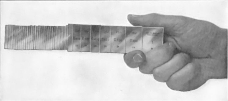
Thirty-six gauges wrung together and held horizontally. (Credit: Goodrich & Stanley, 1907)
As creatures of the macro world, we are largely only aware of the macro effects of the various forces at play around us. We mostly understand gravity, and how the friction of our hand against a glass prevents it from sliding out of our hand before shattering into many pieces on the floor. Yet add some water on the skin of our hands, and suddenly there’s not enough friction, leading to unfortunate glass slippage, or a lid on a jar of pickles that stubbornly refuses to open because we cannot generate enough friction until we manage to dry our hands sufficiently.
Many of these macro-level interactions are the result of molecular-level interactions, which range from the glass staying in one piece instead of drifting off as a cloud of atoms, to the system property that we refer to as ‘friction‘, which itself is also subdivided into static stiction and dynamic friction. The system of friction can be considered to be analogous to contact binding when we consider two plates with one placed on top of the other. If we proceed to change the angle of these stacked plates, at some point the top plate will slide off the bottom plate. This is the point where the binding forces can no longer compensate for the gravitational pull, with material type and surface finish affecting the final angle.
An interesting example of how much surface smoothness matters can be found in gauge blocks. These are precision ground and lapped blocks of metal or ceramic which match a specific thickness. Used for mainly calibration purposes, they posses the fascinating property due to their smooth surfaces that you can make multiple of them adhere together in a near-permanent manner in what is called wringing. This way you can combine multiple lengths to create a single gauge block with sub-millimeter accuracy.
Enabling all this are intermolecular forces, in particular the Van der Waals forces, including dipole-dipole electrostatic interactions. These do not rely on chemical or similar properties as they depend only on aspects like the mutual repulsion between the electron clouds of the atoms that make up the materials involved. Although these forces are very weak and drop off rapidly with distance, they are generally independent of aspects like temperature.
Hydrogen bonds can also occur if present, with each type of force having its own set of characteristics in terms of strength and effective distance.
Make It Smooth
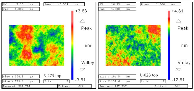
Surface roughnesses of a SiO2 wafer (left, ≈1.01 nm RMS) and an ULE wafer (right, ≈1.03 nm RMS) (Credit: Kalkowski et al., 2011)
One does not simply polish a surface to a nanometer-perfect sheen, though as computer cooling enthusiasts and kin are aware, you can get pretty far with a smooth surface and various grits of sandpaper all the way up to ridiculously high levels. Giving enough effort and time, you can match the surface finish of something like gauge blocks and shave off another degree or two on that CPU at load.
Achieving even smoother surfaces is essentially taking this to the extreme, though it can be done without 40,000 grit sandpaper as well. The easiest way is probably found in glass and optics production, the latter of which has benefited immensely from the semiconductor industry. A good demonstration of this can be found in a 2011 paper (full PDF) by Fraunhofer researchers G. Kalkowski et al. as published in Optical Manufacturing and Testing.
They describe the use of optical contact bonding in the context of glass-glass for optical and precision engineering, specifically low-expansion fused silica (SiO2) and ultra-low expansion materials. There is significant overlap between semiconductor wafers and the wafers used here, with the same nanometer level precision, <1 nm RMS surface roughness, a given. Before joining, the surfaces are extensively cleaned of any contaminants in a vacuum environment.
Worse Than Superglue
Once the surfaces are prepared, there comes the tricky part of making both sides join together. Unlike with the gauge blocks, these super smooth surfaces will not come apart again without a fight, and there’s no opportunity to shimmy them around to get that perfect fit like when using adhesive. With the demonstrated method by Kalkowski et al., the wafers were joined followed by heating to 250 ℃ to create permanent Si-O-Si bonds between the two surfaces. In addition bonding pressure was applied for two hours at 2 MPa using either N2 or O2 gas.
This also shows another aspect of optical contact binding: although it’s not technically permanent, the bond is still just using intermolecular forces, and, as shown in this study, can be pried apart with a razorblade and some effort. By heating and applying pressure, the two surfaces can be annealed, forming molecular bonds and effectively turning the two parts into one.
Of course, there are many more considerations, such as the low-expansion materials used in the referenced study. If both sides use too dissimilar materials, the bond will be significantly more tenuous than if the materials with the same expansion properties are used. It’s also possible to use chemically activated direct bonding with a chemical activation process, all of which relies on the used materials.
In summary, optical contact bonding is a very useful technique, though you may want to have a well-equipped home lab if you want to give it a spin yourself.
With the ability to independently adjust the thrust of each of their four motors, quadcopters are exceptionally agile compared to more traditional aircraft. But in an effort to create an even more maneuverable drone platform, a group of South Korean researchers have studied adding flying squirrel tech to quadcopters. Combined with machine learning, this is said to significantly increase the prototype’s agility in an obstacle course.
Flying squirrels (tribe Pteromyini)) have large skin flaps (patagium) between their wrists and ankles which they use to control their flight when they glide from tree to tree, along with their fluffy squirrel tail. With flights covering up to 90 meters, they also manage to use said tail and patagium to air brake, which prevents them from smacking with bone jarring velocities into a tree trunk.
By taking these principles and adding a similar mechanism to a quadcopter for extending a patagium-like membrane between its rotors, the researchers could develop a new controller (thrust-wing coordination control, TWCC), which manages the extending of the membranes in coordination with thrust from the brushless motors. Rather than relying on trial-and-error to develop the controller algorithms, the researchers trained a recurrent neural network (RNN) which was pre-trained prior to first flights using simulation data followed by supervised learning to refine the model.
During experiments with obstacle avoidance on a test-track, the RNN-based controller worked quite well compared to a regular quadcopter. A disadvantage is of course that the range of these flying squirrel drones is less due to the extra weight and drag, but if one were to make flying drones that will perch on surfaces between dizzying feats of agility in the air, this type of drone tech might just be the ticket.
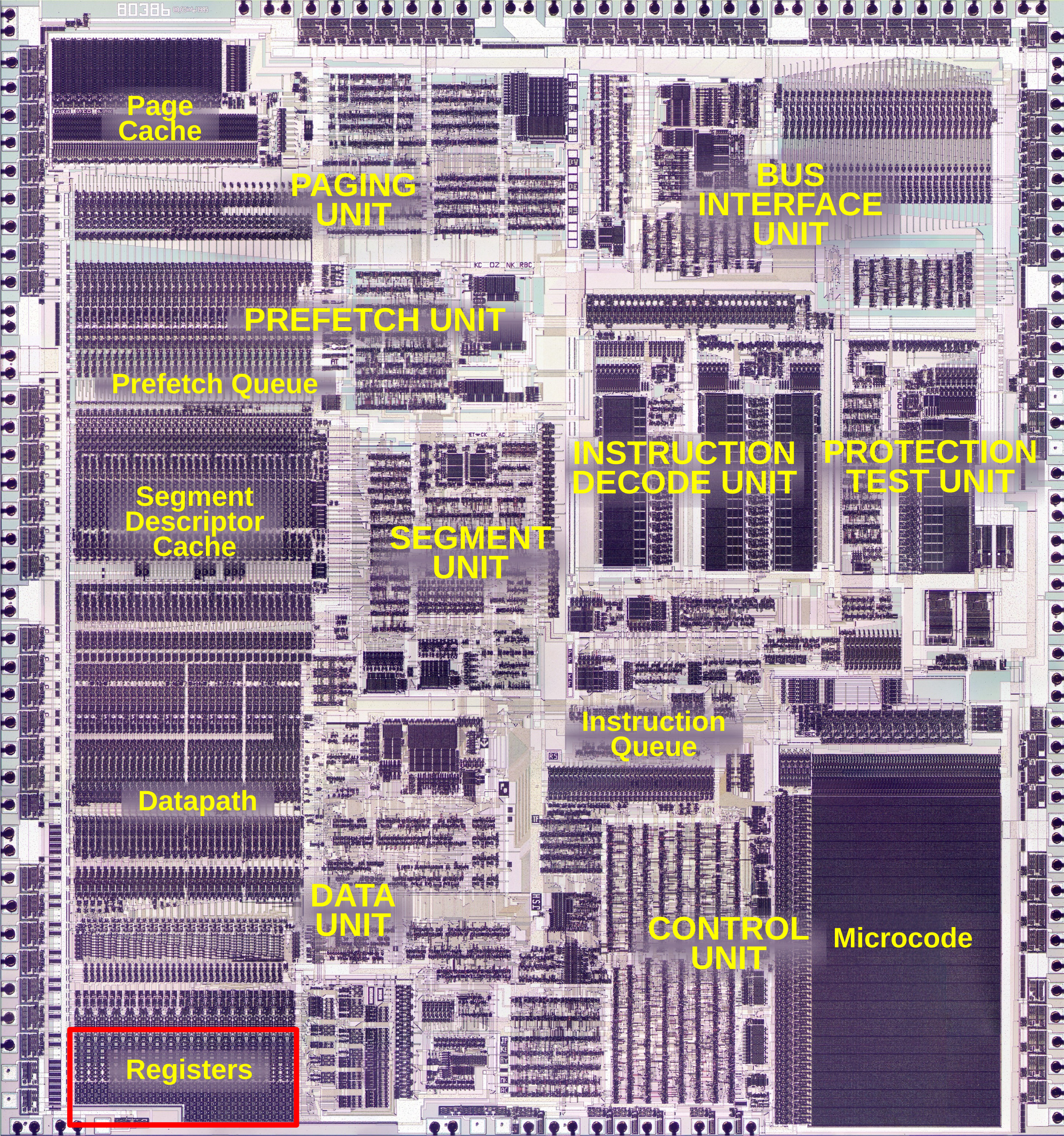
The fact that modern-day x86 processors still pretty much support the same operating systems and software as their ancestors did is quite a feat. Much of this effort had already been accomplished with the release of the 80386 (later 386) CPU in 1985, which was not only the first 32-bit x86 CPU, but was also backwards compatible with 8- and 16-bit software dating back to the 1970s. Making this work transparently was anything but straightforward, as [Ken Shirriff]’s recent analysis of the 80386’s main register file shows.
Labelled Intel 80386 die shot. (Credit: Ken Shirriff)
Using die shots of the 386’s registers and surrounding silicon, it’s possible to piece together how backwards compatibility was implemented. The storage cells of the registers are implemented using static memory (SRAM) as is typical, with much of the register file triple-ported (two read, one write).
Most interestingly is the presence of different circuits (6) to support accessing the register file for 8-, 16- or 32-bit writes and reads. The ‘shuffle’ network as [Ken] calls it is responsible for handling these distinct writes and reads, which also leads to the finding that the bottom 16 bits in the registers are actually interleaved to make this process work smoother.
Fortunately for Intel (and AMD) engineers, this feat wouldn’t have to be repeated again with the arrival of AMD64 and x86_64 many years later, when the 386’s mere 275,000 transistors on a 1 µm process would already be ancient history.
We’ve all seen those cheap bench power supply units (PSUs) for sale online, promising specifications that would cost at least a hundred dollars or more if it were a name brand model. Just how much of a compromise are these (usually rebranded) PSUs, and should you trust them with your electronics? Recently [Denki Otaku] purchased a cheap unit off Amazon Japan for a closer look, and found it to be rather lacking.
Internals of the cheap bench PSU reviewed by Denki Otaku on YouTube.
Major compromises include the lack of an output power switch, no way to check the set current limit without shorting the output, very slow drop in output voltage while adjusting due to the lack of a discharge circuit, and other usability concerns. That’s when the electrical performance of the PSU got tested.
Right off the bat a major issue in this cheap switching mode PSU is clear, as it has 200 mV peak-to-peak noise on its output, meaning very little output filtering. The maximum power output rating was also far too optimistic, with a large voltage drop observed. Despite this, it generally worked well, and the internals – with a big aluminium plate as heatsink – look pretty clean with an interesting architecture.
The general advice is to get a bench PSU that has features like an output power button and an easy way to set the voltage and current limits. Also do not connect it to anything that cares about noise and ripple unless you know that it produces clean, filtered output voltages.