The 2025 Iberian Peninsula Blackout: From Solar Wobbles to Cascade Failures
Some Mondays are worse than others, but April 28 2025 was particularly bad for millions of people in Spain and Portugal. Starting just after noon, a number of significant grid oscillations occurred which would worsen over the course of minutes until both countries were plunged into a blackout. After a first substation tripped, in the span of only a few tens of seconds the effects cascaded across the Iberian peninsula as generators, substations, and transmission lines tripped and went offline. Only after the HVDC and AC transmission lines at the Spain-France border tripped did the cascade stop, but it had left practically the entirety of the peninsula without a functioning power grid. The event is estimated to have been the biggest blackout in Europe ever.
Following the blackout, grid operators in the affected regions scrambled to restore power, while the populace tried to make the best of being plummeted suddenly into a pre-electricity era. Yet even as power gradually came back online over the course of about ten hours, the question of what could cause such a complete grid collapse and whether it might happen again remained.
With recently a number of official investigation reports having been published, we have now finally some insight in how a big chunk of the European electrical grid suddenly tipped over.
Oscillations
Electrical grids are a rather marvelous system, with many generators cooperating across thousands of kilometers of transmission lines to feed potentially millions of consumers, generating just enough energy to meet the amount demanded without generating any more. Because physical generators turn more slowly when they are under heavier load, the frequency of the AC waveform has been the primary coordination mechanism across power plants. When a plant sees a lower grid frequency, it is fueled up to produce more power, and vice-versa. When the system works well, the frequency slowly corrects as more production comes online.
The greatest enemy of such an interconnected grid is an unstable frequency. When the frequency changes too quickly, plants can’t respond in time, and when it oscillates wildly, the maximum and minumum values can exceed thresholds that shut down or disconnect parts of the power grid.
In the case of the Iberian blackout, a number of very significant oscillations were observed in the Spanish and Portuguese grids that managed to also be observable across the entire European grid, as noted in an early analysis (PDF) by researchers at Germany’s Friedrich-Alexander-Universität (FAU).
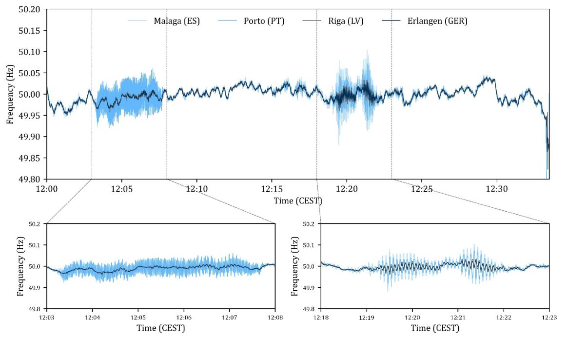
This is further detailed in the June 18th report (direct PDF link) by Spain’s Transmission System Operator (TSO) Red Eléctrica (REE). Much of that morning the grid was plagued by frequency oscillations, with voltage increases occurring in the process of damping said oscillations. None of this was out of the ordinary until a series of notable events, with the first occurring after 12:02 with an 0.6 Hz oscillation repeatedly forced by a photovoltaic (PV) solar plant in the province of Badajoz which was feeding in 250 MW at the time. After stabilizing this PV plant the oscillation ceased, but this was followed by the second event with an 0.2 Hz oscillation.
After this new oscillation was addressed through a couple of measures, the grid was suffering from low-voltage conditions caused by the oscillations, making it quite vulnerable. It was at this time that the third major event occurred just after 12:32, when a substation in Granada tripped. The speculation by REE being that its transformer tap settings had been incorrectly set, possibly due to the rapidly changing grid conditions outpacing its ability to adjust.
Subsequently more substations, solar- and wind farms began to go offline, mostly due to a loss of reactive power absorption causing power flow issues, as the cascade failure outpaced any isolation attempts and conventional generators also threw in the towel.
Reactive Power
Grid oscillations are a common manifestation in any power grid, but they are normally damped either with no or only minimal interaction required. As also noted in the earlier referenced REE report, a big issue with the addition of solar generators on the grid is that these use grid-following inverters. Unlike spinning generators that have intrinsic physical inertia, solar inverters can rapidly follow the grid voltage and thus do not dampen grid oscillations or absorb reactive power. Because they can turn on and off essentially instantaneously, these inverters can amplify oscillations and power fluctuations across the grid by boosting or injecting oscillations if the plants over-correct.
In alternating current (AC) power systems, there are a number of distinct ways to describe power flow, including real power (Watt), complex power (VA) and reactive power (var). To keep a grid stable, all of these have to be taken into account, with the reactive power management being essential for overall stability. With the majority of power at the time of the blackout being generated by PV solar farms without reactive power management, the grid fluctuations spun out of control.
Generally, capacitors are considered to create reactive power, while inductors absorb it. This is why transformer-like shunt reactors – a parallel switchyard reactor – are an integral part of any modern power grid, as are the alternators at conventional power plants which also absorb reactive power through their inertia. With insufficient reactive power absorption capacity, damping grid oscillations becomes much harder and increases the chance of a blackout.
Ultimately the cascade failure took the form of an increasing number of generators tripping, which raised the system voltage and dropped the frequency, consequently causing further generators and transmission capacity to trip, ad nauseam. Ultimately REE puts much of the blame at the lack of reactive power which could have prevented the destabilization of the grid, along with failures in voltage control. On this Monday PV solar in particular generated the brunt of grid power in Spain at nearly 60%.
Not The First Time
Despite the impression one might get, this wasn’t the first time that grid oscillations have resulted in a blackout. Both of the 1996 Western North America blackouts involved grid oscillations and a lack of reactive power absorption, and the need to dampen grid oscillations remains one of the highest priorities. This is also where much of the criticism directed towards the current Spanish grid comes from, as the amount of reactive power absorption in the system has been steadily dropping with the introduction of more variable renewable energy (VRE) generators that lack such grid-stabilizing features.
To compensate for this, wind and solar farms would have to switch to grid-forming inverters (GFCs) – as recommended by the ENTSO-E in a 2020 report – which would come with the negative effect of making VREs significantly less economically viable. Part of this is due to GFCs still being fairly new, while there is likely a strong need for grid-level storage to be added to any GFC in order to make especially Class 3 fully autonomous GFCs work.
It is telling that five years after the publication of this ENTSO-E report not much has changed, and GFCs have not yet made inroads as a necessity for stable grid operation. Although the ENTSO-E’s own investigation is still in progress with a final report not expected for a few more months at least, in light of the available information and expert reports, it would seem that we have a good idea of what caused the recent blackout.
The pertinent question is thus more likely to be what will be done about it. As Spain and Portugal move toward a power mix that relies more and more heavily on solar generation, it’s clear that these generators will need to pick up the slack in grid forming. The engineering solution is known, but it is expensive to retrofit inverters, and it’s possible that this problem will keep getting kicked down the road. Even if all of the reports are unanimous in their conclusion as to the cause, there are unfortunately strong existing incentives to push the responsibility of avoiding another blackout onto the transmission system operators, and rollout of modern grid-forming inverters in the solar industry will simply take time.
In other words, better get used to more blackouts and surviving a day or longer without power.