As practical SD cards are, they lack much of what made floppy disks and cartridges so awesome: room for art and a list of contents, as well as the ability to not be lost in shaggy carpet or down a pet’s gullet. In a fit of righteous nostalgia, [Abe] decided that he’d turn SD cards into cartridges in the best way possible, and amazingly managed to not only finish the project after two years, but also make it look snazzy enough to have come straight out of the 1980s. The resulting cartridges come both with fixed (256 MB) and removable micro SD card storage, which are mounted on a PCB that passively connects to pogo pins in the custom, 3D printed reader.
Front of an SD-card-turned-cartridge with adn without decal. (Credit: Abe’s Projects, YouTube)
The inspiration for this project kicked in while [Abe] was working on a floppy drive conversion project called the Floppy8, which crammed an MCU into an external floppy drive along with a rough version of these SD card-based cartridges that used the physical card’s edge connector to connect with a micro SD slot inside the converted floppy drive. The problem with this setup was that alignment was terrible, and micro SD cards would break, along with a range of other quality of life issues.
Next, the SD card was put into a slot on the carrier PCB that featured its own edge connector. This improved matters, but the overly complicated (moving) read head in the reader turned out to be very unreliable, in addition to FDM printed parts having general tolerance and durability issues. Eventually a simplified design which takes these limitations in mind was created that so far seems to work just fine.
Although SD cards in cartridges are not a new idea, using them purely as a data carrier is far less common. One could argue about the practicality of turning a fingernail-sized micro SD card into something much larger, but in terms of aesthetics and handleability it definitely gets an A+.
Although commonly referred to as a ‘timer IC’, the venerable NE555 and derivatives are in fact not timer ICs. This perhaps controversial statement is the open door that gets kicked in by [PKAE Electronics] over at YouTube, as he explains with excellent diagrams and simulations how exactly these ICs work, and what it takes to make it actually do timer things. For anyone who has ever used one of these chips there is probably nothing too mind-blowing, but it’s an infinitely better way to wrap your way around an NE555 and kin than a datasheet.
At its core, the 555 contains three 5 kOhm resistors as a voltage divider, which has been incorrectly postulated to be the source of the chip’s name. This voltage divider controls two comparators, which in turn control an SR flipflop. These comparators are used for the voltage trigger and threshold inputs, which in turn toggle the flipflop, respectively setting and resetting it. This by itself just means that the 555 can be used as a threshold detector, with settable control voltage. How a 555 becomes a timer is when the discharge, trigger and threshold pins are combined with external resistors and a capacitor, which creates a smooth square wave on the 555’s output pin.
There are many ways to make basic components into an oscillator of some type, but the 555 is a great choice when you want something more refined that doesn’t involve using an entire MCU. That said, there’s far more that the 555 can be used for, as [PKAE] alludes to, and we hope that he makes more excellent videos on these applications.
When thinking about loops in programming languages, they often get simplified down to a conditions section and a body, but this belies the dizzying complexity that emerges when considering loop edge cases within the context of static analysis. A paper titled Misconceptions about Loops in C by [Martin Brain] and colleagues as presented to SOAP 2024 conference goes through a whole list of false assumptions when it comes to loops, including for languages other than C. Perhaps most interesting is the conclusion that these ‘edge cases’ are in fact a lot more common than generally assumed, courtesy of how creative languages and their users can be when writing their code, with or without dragging in the meta-language of C’s preprocessor.
Assumptions like loop equivalence can fall apart when considering the CFG ( control flow graph) interpretation versus a parse tree one where the former may e.g. merge loops. There are also doozies like assuming that the loop body will always exist, that the first instruction(s) in a loop are always the entry point, and the horrors of estimating loop exits in the context of labels, inlined functions and more. Some languages have specific loop control flow features that differ from C (e.g. Python’s for/else and Ada’s loop), all of which affect a static analysis.
Ultimately, writing a good static analysis tool is hard, and there are plenty of cases where it’s likely to trip up and give an invalid result. A language which avoids ambiguity (e.g. Ada) helps immensely here, but for other languages it helps to write your code as straightforward as possible to give the static analysis tool a fighting chance, or just get really good at recognizing confused static analysis tool noises.
(Heading image: Control flow merges can create multiple loop entry
edges (Credit: Martin Brand, et al., SOAP 2024) )
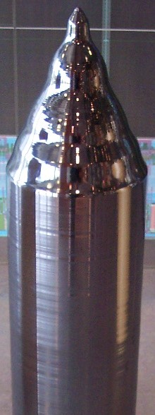
Die photo of the Intel Pentium processor with standard cells highlighted in red. The edges of the chip suffered some damage when I removed the metal layers. (Credit: Ken Shirriff)
Whereas the CPUs and similar ASICs of the 1970s had their transistors laid out manually, with the move from LSI to VLSI, it became necessary to optimize the process of laying out the transistors and the metal interconnects between them. This resulted in the development of standard-cells: effectively batches of transistors with each a specific function that could be chained together. First simple and then more advanced auto-routing algorithms handled the placement and routing of these standard elements, leading to dies with easily recognizable structures under an optical microscope. Case in point an original (P54C) Intel Pentium, which [Ken Shirriff] took an in-depth look at.
Using a by now almost unimaginably large 600 nm process, the individual elements of these standard cells including their PMOS and NMOS components within the BiCMOS process can be readily identified and their structure reverse-engineered. What’s interesting about BiCMOS compared to CMOS is that the former allows for the use of bipolar junction transistors, which offer a range of speed, gain and output impedance advantages that are beneficial for some part of a CPU compared to CMOS. Over time BiCMOS’ advantages became less pronounced and was eventually abandoned.
All in all, this glimpse at the internals of a Pentium processor provides a fascinating snapshot of high-end Intel semiconductor prowess in the early 1990s.
(Top image: A D flip-flop in the Pentium. Credit: [Ken Shirriff] )
The late 1990s saw the widespread introduction of solid-state storage based around NAND Flash. Ranging from memory cards for portable devices to storage for desktops and laptops, the data storage future was prophesied to rid us of the shackles of magnetic storage that had held us down until then. As solid-state drives (SSDs) took off in the consumer market, there were those who confidently knew that before long everyone would be using SSDs and hard-disk drives (HDDs) would be relegated to the dust bin of history as the price per gigabyte and general performance of SSDs would just be too competitive.
Fast-forward a number of years, and we are now in a timeline where people are modifying SSDs to have less storage space, just so that their performance and lifespan are less terrible. The reason for this is that by now NAND Flash has hit a number of limits that prevent it from further scaling density-wise, mostly in terms of its feature size. Workarounds include stacking more layers on top of each other (3D NAND) and increasing the number of voltage levels – and thus bits – within an individual cell. Although this has boosted the storage capacity, the transition from single-level cell (SLC) to multi-level (MLC) and today’s TLC and QLC NAND Flash have come at severe penalties, mostly in the form of limited write cycles and much reduced transfer speeds.
So how did we get here, and is there life beyond QLC NAND Flash?
Floating Gates
Basic model of a floating-gate transistor.
At the core of NAND Flash lies the concept of floating gates, as first pioneered in the 1960s with the floating-gate MOSFET (FGMOS). As an FGMOS allows for the retention of a charge in the floating gate, it enabled the development of non-volatile semiconductor storage technologies like EPROM, EEPROM and flash memory. With EPROM each cell consists out of a single FET with the floating and control gates. By inducing hot carrier injection (HCI) with a programming voltage on the control gate, electrons are injected into the floating gate, which thus effectively turns the FET on. This allows then for the state of the transistor to be read out and interpreted as the stored bit value.
Naturally, just being able to program an EPROM once and then needing to erase the values by exposing the entire die to UV radiation (to induce ionization within the silicon oxide which discharges the FET) is a bit of a bother, even if it allowed the chip to be rewritten thousands of times. In order to make EPROMs in-circuit rewritable, EEPROMs change the basic FET-only structure with two additional transistors. Originally EEPROMs used the same HCI principle for erasing a cell, but later they would switch to using Fowler-Nordheim tunneling (FNT, the wave-mechanical form of field electron emission) for both erasing and writing a cell, which removes the damaging impact of hot carrier degradation (HCD). HCD and the application of FNT are both a major source of the physical damage that ultimately makes a cell ‘leaky’ and rendering it useless.
Combined with charge trap flash (CTF) that replaces the original polycrystalline silicon floating gate with a more durable and capable silicon nitride material, modern EEPROMs can support around a million read/write cycles before they wear out.
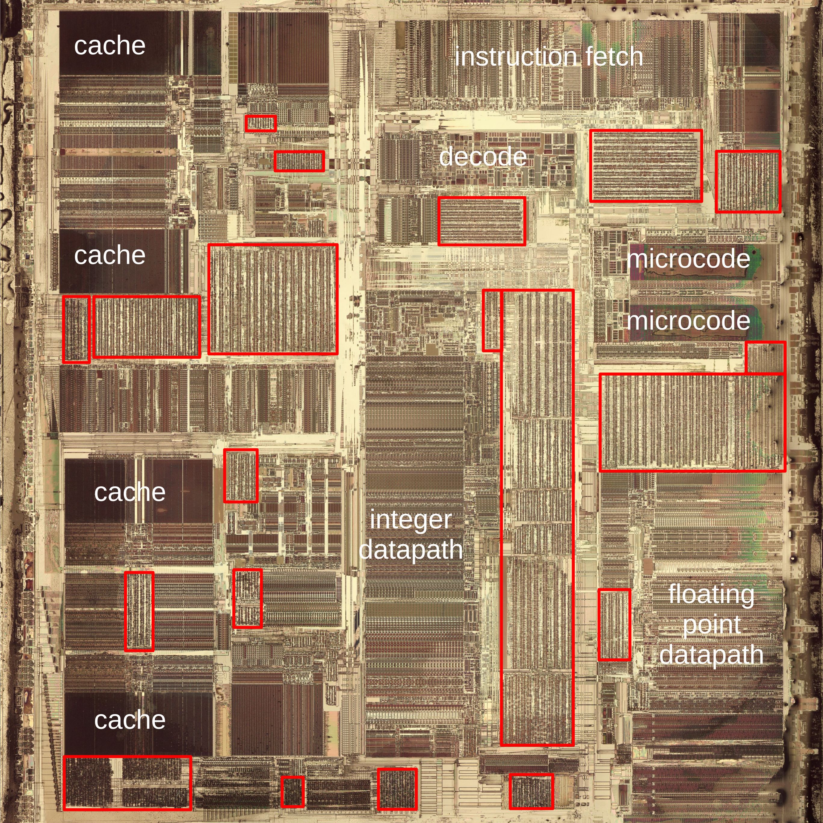
Flash memory is a further evolution of the EEPROM, with the main distinctions being a focus on speed and high storage density, as well as the use of HCI for writes in NOR Flash, due to the speed benefits this provides. The difference between NOR and NAND Flash comes from the way in which the cells are connected, with NOR Flash called that way because it resembles a NOR gate in its behavior:
NOR flash memory wiring and structure on silicon (Credit: Cyferz, Wikimedia)
To write a NOR Flash cell (set it to logical ‘0’), an elevated voltage is applied to the control gate, inducing HCI. To erase a cell (reset to logical ‘1’), a large voltage of opposite polarity is applied to the control gate and the source terminal, which draws electrons out of the floating gate due to FNT.
Reading a cell is then performed by pulling the target word line high. Since all of the storage FETs are connected to both ground and the bit line, this will pull the bit line low if the floating gate is active, creating a logical ‘1’ and vice versa. NOR Flash is set up to allow for bit-wise erasing and writing, although modern NOR Flash is moving to a model in which erasing is done in blocks, much like with NAND Flash:
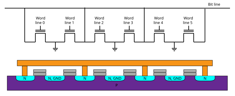
NAND flash memory wiring and structure on silicon (Credit: Cyferz, Wikimedia)
The reason why NAND Flash is called this way is readily apparent from the way the cells are connected, with a number of cells connected in series (a string) between the bit line and ground. NAND Flash uses FNT for both writing and erasing cells, which due to its layout always has to be written (set to ‘0’) and read in pages (a collection of strings), while erasing is performed on a block level (a collection of pages).
Unlike NOR Flash and (E)EPROM, the reading out of a value is significantly more complicated than toggling a control gate and checking the level of the bit line. Instead the control gate on a target cell has to be activated, while putting a much higher (>6V) voltage on the control gate of unwanted cells in a string (which turns them on no matter what). Depending on the charge inside the floating gate, the bit line voltage will reach a certain level, which can then be interpreted as a certain bit value. This is also how NAND Flash can store multiple bits per cell, by relying on precise measurements of the charge level of the floating gate.
All of this means that while NOR Flash supports random (byte-level) access and erase and thus eXecute in Place (XiP, allows for running applications directly off ROM), NAND Flash is much faster with (block-wise) writing and erasing, which together with the higher densities possible has led to NAND Flash becoming the favorite for desktop and mobile data storage applications.
Scaling Pains
With the demand for an increasing number of bytes-per-square-millimeter for Flash storage ever present, manufacturers have done their utmost to shrink the transistors and other structures that make up a NAND Flash die down. This has led to issues such as reduced data retention due to electron leakage and increased wear due to thinner structures. The quick-and-easy way to bump up total storage size by storing more bits per cell has not only exacerbated these issues, but also introduced significant complexity.
The increased wear can be easily observed when looking at the endurance rating (program/erase (P/E) cycles per block) for NAND Flash, with SLC NAND Flash hitting up to 100,000 P/E cycles, MLC below 10,000, TLC around a thousand and QLC dropping down to hundreds of P/E cycles. Meanwhile the smaller feature sizes have made NAND Flash more susceptible to electron leakage from electron mobility, such from high environmental temperatures. Data retention also decreases with wear, making data loss increasingly more likely with high-density, multiple bits per cell NAND Flash.
Because of the complexity of QLC NAND Flash with four bits (and thus 16 voltage levels) per cell, the write and read speeds have plummeted compared to TLC and especially SLC. This is why QLC (and TLC) SSDs use a pseudo-SLC (pSLC) cache, which allocates part of the SSD’s Flash to be only used only with the much faster SLC access pattern. In the earlier referenced tutorial by Gabriel Ferraz this is painfully illustrated by writing beyond the size of the pSLC cache of the target SSD (a Crucial BX500):
(Credit: Gabriel Ferraz)
Although the writes to the target SSD are initially nearly 500 MB/s, the moment the ~45 GB pSLC cache fills up, the write speeds are reduced to the write speeds of the underlying Micron 3D QLC NAND, which are around 50 MB/s. Effectively QLC NAND Flash is no faster than a mechanical HDD, and with worse data retention and endurance characteristics. Clearly this is the point where the prophesied solid state storage future comes crumbling down as even relatively cheap NAND Flash still hasn’t caught up to the price/performance of HDDs.
(Credit: Gabriel Ferraz)
The modification performed by Gabriel Ferraz on the BX500 SSD involves reprogramming its Silicon Motion SM2259XT2 NAND Flash controller using the MPTools software, which is not provided to consumers but has been leaked onto the internet. While not as simple as toggling on a ‘use whole SSD as pSLC’ option, this is ultimately what it comes down to after flashing modified firmware to the drive.
With the BX500 SSD now running in pSLC mode, it knocks the storage capacity down from 500 GB to 120 GB, but the P/E rating goes up from a rated 900 cycles in QLC mode to 60,000 cycles in pSLC mode, or well over 3,000%. The write performance is a sustained 496 MB/s with none of the spikes seen in QLC mode, leading to about double the score in the PCMark 10 Full System Drive test.
With all of this in mind, it’s not easy to see a path forward for NAND Flash which will not make these existing issues even worse. Perhaps Intel and Micron will come out of left field before long with a new take on the 3D XPoint phase-change memory, or perhaps we’ll just keep muddling on for the foreseeable future with ever worse SSDs and seemingly immortal HDDs.
Clearly one should never believe prophets, especially not those for shiny futuristic technologies.
With both of the dominant display technologies today – LCD and OLED – being far from perfect, there is still plenty of room in the market for the Next Big Thing. One of the technologies being worked on is called PeLED, for Perovskite LED. As a semiconductor material, it can both be induced to emit photons as well as respond rather strongly to incoming photons. That is a trick that today’s displays haven’t managed without integrating additional sensors. This technology could be used to create e.g. touch screens without additional hardware, as recently demonstrated by [Chunxiong Bao] and colleagues at Linköping University in Sweden and Nanjing University in China.
Their paper in Nature Electronics describes the construction of photo-responsive metal halide perovskite pixels, covering the typical red (CsPbI3−xBrx), green (FAPbBr3), and blue (CsPbBr3−xClx) wavelengths. The article also describes the display’s photo-sensing ability to determine where a finger is placed on the display. In addition, it can work as an ambient light sensor, a scanner, and a solar cell to charge a capacitor. In related research by [Yun Gao] et al. in Nature Electronics, PeLEDs are demonstrated with 1 microsecond response time.
As usual with perovskites, their lack of stability remains their primary obstacle. In the article by [Chunxiong Bao] et al. the manufactured device with red pixels was reduced to 80% of initial brightness after 18.5 hours. While protecting the perovskites from oxygen, moisture, etc. helps, this inherent instability may prevent PeLEDs from ever becoming commercialized in display technology. Sounds like a great challenge for the next Hackaday Prize!
Most of us would equate commercial airline travel with fixed-wing aircraft, but civilian transport by helicopter, especially in large and sparsely populated regions, is common enough. It was once even big business in the Soviet Union, where the Aeroflot airline operated passenger helicopters in regular service for many decades. In the mid-1960s they even started work on converting the Mil Mi-6 — the USSR’s largest and fastest helicopter — to carry paying passengers. Unfortunately this never got past a single prototype, with the circumstances described by [Oliver Parken] in a recent article.
This passenger version of the Mi-6 got the designation Mi-6P (for passazhirskyi, meaning passenger) and would have seated up to 80 (3 + 2 row configuration), compared to the Mi-8 passenger variant that carried 28 – 31 passengers. Why exactly the Mi-6P never got past the prototype stage is unknown, but its successor in the form of the Mi-26P has a listed passenger variant and features. Both have a cruising speed of around 250 km/h, with a top of 300 km/h. The auxiliary winglets of the Mi-6 provided additional lift during flight, and the weight lifting record set by the Mi-6 was only broken by the Mi-26 in 1982.
An obvious disadvantage of passenger helicopters is that they are more complicated to operate and maintain, while small fixed wing airliners like the ATR 72 (introduced in 1988) can carry about as many passengers, requires just a strip of tarmac to land and take off from, travel about twice as fast as an Mi-6P would, and do not require two helicopter pilots to fly them. Unless the ability to hover and land or take-off vertically are required, this pretty much explains why passenger helicopters are such a niche application. Not that the Mi-6P doesn’t have that certain je ne sais quoi to it, mind.
One of the fun parts of the ESP32-S3 microcontroller is that it got upgraded to the newer Cadence Xtensa LX7 processor core, which turns out to have a range of SIMD instructions that can help to significantly speed up a range of tasks. [Shranav Palakurthi] recently used this to speed up the processing of video frames to detect corners using the FAST method. By moving some operations that benefit from SIMD over to an optimized version written in LX7 ASM, the algorithm’s throughput was increased by 220%, from 5.1 MP/s to 11.2 MP/s, albeit with some caveats.
The problem with the SIMD instructions in the LX7 other than them being very poorly documented – unless you sign an NDA with Cadence – is that it misses many instructions that would be really useful. For [Shranav] the lack of support for direct misaligned reads and comparing of unsigned 8-bit numbers were hurdles, but could be worked around, with the results available on GitHub.
Much of the groundwork for this SIMD implementation was laid by [Larry Bank], who reverse-engineered the SIMD instructions from available documentation and code samples, finding that the ESP32-S3 misses quite a few common SIMD instructions, including various shifts and unaligned reads and writes. Still, it’s good enough for quite a few tasks, as long as you can make it work with the available instructions.
In the communications surrounding LLMs and popular interfaces like ChatGPT the term ‘hallucination’ is often used to reference false statements made in the output of these models. This infers that there is some coherency and an attempt by the LLM to be both cognizant of the truth, while also suffering moments of (mild) insanity. The LLM thus effectively is treated like a young child or a person suffering from disorders like Alzheimer’s, giving it agency in the process. That this is utter nonsense and patently incorrect is the subject of a treatise by [Michael Townsen Hicks] and colleagues, as published in Ethics and Information Technology.
Much of the distinction lies in the difference between a lie and bullshit, as so eloquently described in [Harry G. Frankfurt]’s 1986 essay and 2005 book On Bullshit. Whereas a lie is intended to deceive and cover up the truth, bullshitting is done with no regard for, or connection with, the truth. The bullshitting is only intended to serve the immediate situation, reminiscent of the worst of sound bite culture.
When we consider the way that LLMs work, with the input query used to provide a probability fit across the weighted nodes that make up its vector space, we can see that the generated output is effectively that of an oversized word prediction algorithm. This precludes any possibility of intelligence and thus cognitive awareness of ‘truth’. Meaning that even if there is no intent behind the LLM, it’s still bullshitting, even if it’s the soft (unintentional) kind. When taking into account the agency and intentions of those who created the LLM, trained it, and created the interface (like ChatGPT), however, we enter into hard, intentional bullshit territory.
It is incidentally this same bullshitting that has led to LLMs being partially phased out already, with Retrieval Augmented Generation (RAG) turning a word prediction algorithm into more of a fancy search machine. Even venture capitalists can only take so much bullshit, after all.
As a result of the European Union’s push for greater repairability of consumer devices like smartphones, Apple sees itself forced to make the batteries in the iPhone user-replaceable by 2027. Reportedly, this has led Apple to look at using electroadhesion rather than conventional adhesives which require either heat, isopropyl alcohol, violence, or all of the above to release. Although details are scarce, it seems that the general idea would be that the battery is wrapped in metal, which, together with the inside of the metal case, would allow for the creation of a cationic/anionic pair capable of permanent adhesion with the application of a low-voltage DC current.
This is not an entirely wild idea. Tesa has already commercialized it in the electrical debonding form of its Debonding on Demand product. This uses a tape that’s applied to one side of the (metal) surfaces, with a 5 bar pressure being applied for 5 seconds. Afterwards, the two parts can be released again without residue as shown in the above image. This involves applying a 12V DC voltage for 60 seconds, with the two parts afterward removable without force.
Tesa markets this right alongside the pull tab adhesive strips which are currently all the rage in smartphones, with the opinions on pull strips during battery replacement strongly divided. A bottle of IPA is always good to have nearby when a pull tab inevitably snaps off and you have to pry the battery loose. In that regard electroadhesion for debonding would make life significantly easier since the times when batteries were not a structural part of smartphones are unlikely to return no matter how much we might miss them.
We covered electroadhesion previously, as you can make just about anything stick to anything, including biological tissues to graphite and metal, with potentially interesting applications in robotics and medicine.
Showing off the 3D-printed hydraulics system. (Credit: Indeterminate Design, YouTube)
Hydraulics are incredibly versatile, but due to the pressures at which they operate, they are also rather expensive and not very DIY-friendly. This isn’t to say that you cannot take a fair shot at a halfway usable 3D-printed set of hydraulics, as [Indeterminate Design] demonstrates in a recent video. Although not 100% 3D-printed, it does give a good idea of how far you can push plastic-based additive manufacturing in this field.
Most interesting is the integration of the gear pump, 4-way selector valve, and relief valve into a single structure, which was printed with a resin printer (via the JLC3DP 3D print service). After bolting on the (also 3D printed) clear reservoir and assembling the rest of the structure including the MR63 ball bearings, relief spring valve, and pneumatic fittings it was ready to be tested. The (unloaded) gear pump could pump about 0.32 L/minute, demonstrating its basic functionality.
For the hydraulic cylinder, mostly non-3D printed parts were used, with a brass cylinder forming the main body. During these initial tests, plain water was used, followed by CHF11 hydraulic oil, with a pressure of about 1.3 bar (19 PSI) calculated afterward. This fairly low pressure is suspected to be caused by leaky seals (including the busted shaft seal), but as a basic proof of concept, it provides an interesting foundation for improvements.
Although it’s often said that the era of ocean liners came to an end by the 1950s with the rise of commercial aviation, reality isn’t quite that clear-cut. Coming out of the troubled 1940s arose a new kind of ocean liner, one using cutting-edge materials and propulsion, with hybrid civil and military use as the default, leading to a range of fascinating design decisions. This was the context in which the SS United States was born, with the beating heart of the US’ fastest battle ships, with light-weight aluminium structures and survivability built into every single aspect of its design.
Outpacing the super-fast Iowa-class battleships with whom it shares a lot of DNA due to its lack of heavy armor and triple 16″ turrets, it easily became the fastest ocean liner, setting speed records that took decades to be beaten by other ocean-going vessels, though no ocean liner ever truly did beat it on speed or comfort. Tricked out in the most tasteful non-flammable 1950s art and decorations imaginable, it would still be the fastest and most comfortable way to cross the Atlantic today. Unfortunately ocean liners are no longer considered a way to travel in this era of commercial aviation, leading to the SS United States and kin finding themselves either scrapped, or stuck in limbo.
In the case of the SS United States, so far it has managed to escape the cutting torch, but while in limbo many of its fittings were sold off at auction, and the conservation group which is in possession of the ship is desperately looking for a way to fund the restoration. Most recently, the owner of the pier where the ship is moored in Camden, New Jersey got the ship’s eviction approved by a judge, leading to very tough choices to be made by September.
A Unique Design
WW II-era United States Maritime Commission (MARCOM) poster.
The designer of the SS United States is William Francis Gibbs, who despite being a self-taught engineer managed to translate his life-long passion for shipbuilding into a range of very notable ships. Many of these were designed at the behest of the United States Maritime Commission (MARCOM), which was created by the Merchant Marine Act of 1936, until it was abolished in 1950. MARCOM’s task was to create a merchant shipbuilding program for hundreds of modern cargo ships that would replace the World War I vintage vessels which formed the bulk of the US Merchant Marine. As a hybrid civil and federal organization, the merchant marine is intended to provide the logistical backbone for the US Navy in case of war and large-scale conflict.
The first major vessel to be commissioned for MARCOM was the SS America, which was an ocean liner commissioned in 1939 and whose career only ended in 1994 when it (then named the American Star) wrecked at the Canary Islands. This came after it had been sold in 1992 to be turned into a five-star hotel in Thailand. Drydocking in 1993 had revealed that despite the advanced age of the vessel, it was still in remarkably good condition.
Interestingly, the last merchant marine vessel to be commissioned by MARCOM was the SS United States, which would be a hybrid civilian passenger liner and military troop transport. Its sibling, the SS America, was in Navy service from 1941 to 1946 when it was renamed the USS West Point (AP-23) and carried over 350,000 troops during the war period, more than any other Navy troopship. Its big sister would thus be required to do all that and much more.
Need For Speed
SS United States colorized promotional B&W photograph. The ship’s name and an American flag have been painted in position here as both were missing when this photo was taken during 1952 sea trials.
William Francis Gibbs’ naval architecture firm – called Gibbs & Cox by 1950 after Daniel H. Cox joined – was tasked to design the SS United States, which was intended to be a display of the best the United States of America had to offer. It would be the largest, fastest ocean liner and thus also the largest and fastest troop and supply carrier for the US Navy.
Courtesy of the major metallurgical advances during WW II, and with the full backing of the US Navy, the design featured a military-style propulsion plant and a heavily compartmentalized design following that of e.g. the Iowa-class battleships. This meant two separate engine rooms and similar levels of redundancy elsewhere, to isolate any flooding and other types of damage. Meanwhile the superstructure was built out of aluminium, making it both very light and heavily corrosion-resistant. The eight US Navy M-type boilers (run at only 54% of capacity) and a four-shaft propeller design took lessons learned with fast US Navy ships to reduce vibrations and cavitation to a minimum. These lessons include e.g. the the five- and four-bladed propeller design also seen used with the Iowa-class battleships with their newer configurations.
Another lessons-learned feature was a top to bottom fire-proofing after the terrible losses of the SS Morro Castle and SS Normandie, with no wood, fabrics or other flammable materials onboard, leading to the use of glass, metal and spun-glass fiber, as well as fireproof fabrics and carpets. This extended to the art pieces that were onboard the ship, as well as the ship’s grand piano which was made from mahogany whose inability to ignite was demonstrated by trying to burn it with a gasoline fire.
The actual maximum speed that the SS United States can reach is still unknown, with it originally having been a military secret. Its first speed trial supposedly saw the vessel hit an astounding 43 knots (80 km/h), though after the ship was retired from the United States Lines (USL) by the 1970s and no longer seen as a naval auxiliary asset, its top speed during the June 10, 1952 trial was revealed to be 38.32 knots (70.97 km/h). In service with USL, its cruising speed was 36 knots, gaining it the Blue Riband and rightfully giving it its place as America’s Flagship.
A Fading Star
The SS United States was withdrawn from passenger service by 1969, in a very unexpected manner. Although the USL was no longer using the vessel, it remained a US Navy reserve vessel until 1978, meaning that it remained sealed off to anyone but US Navy personnel during that period. Once the US Navy no longer deemed the vessel relevant for its needs in 1978, it was sold off, leading to a period of successive owners. Notable was Richard Hadley who had planned to convert it into seagoing time-share condominiums, and auctioned off all the interior fittings in 1984 before his financing collapsed.
In 1992, Fred Mayer wanted to create a new ocean liner to compete with the Queen Elizabeth, leading him to have the ship’s asbestos and other hazardous materials removed in Ukraine, after which the vessel was towed back to Philadelphia in 1996, where it has remained ever since. Two more owners including Norwegian Cruise Line (NCL) briefly came onto the scene, but economic woes scuttled plans to revive it as an active ocean liner. Ultimately NCL sought to sell the vessel off for scrap, which led to the SS United States Conservancy (SSUSC) to take over ownership in 2010 and preserve the ship while seeking ways to restore and redevelop the vessel.
Considering that the running mate of the SS United States (the SS America) was lost only a few years prior, this leaves the SS United States as the only example of a Gibbs ocean liner, and a poignant reminder of what would have been a highlight of the US’s marine prowess. Compared to the United Kingdom’s record here, with the Queen Elizabeth 2(QE2, active since 1969) now a floating hotel in Dubai and the Queen Mary 2‘s maiden voyage in 2004, the US looks to be rather meager when it comes to preserving its ocean liner legacy.
End Of The Line?
The curator of the Iowa-class USS New Jersey (BB-62, currently fresh out of drydock), Ryan Szimanski, walked over from his museum ship last year to take a look at the SS United States, which is moored literally within viewing distance from his own pride and joy. Through the videos he made, one gains a good understanding of both how stripped the interior of the ship is, but also how amazingly well-conserved the ship is today. Even after decades without drydocking or in-depth maintenance, the ship looks like could slip into a drydock tomorrow and come out like new a year or so later.
At the end of all this, the question remains whether the SS United States deserves it to be preserved. There are many arguments for why this would the case, from its unique history as part of the US Merchant Marine, its relation to the highly successful SS America, it being effectively a sister ship to the four Iowa-class battleships, as well as a strong reminder of the importance of the US Merchant Marine at some point in time. The latter especially is a point which professor Sal Mercogliano (from What’s Going on With Shipping? fame) is rather passionate about.
Currently the SSUSC is in talks with a New York-based real-estate developer about a redevelopment concept, but this was thrown into peril when the owner of the pier suddenly doubled the rent, leading to the eviction by September. Unless something changes for the better soon, the SS United States stands a good chance of soon following the USS Kitty Hawk, USS John F. Kennedy (which nearly became a museum ship) and so many more into the scrapper’s oblivion.
What, one might ask, is truly in the name of the SS United States?
After the Living Computers museum in Seattle closed like so many museums and businesses in 2020 with the pandemic, there were many who feared that it might not open again. Four years later this fear has become reality, as the Living Computers: Museum + Labs (LCM+L, for short) entire inventory is being auctioned off. This occurs only 12 years after the museum and associated educational facilities were opened to the public. Along with Allen’s collection at the LCM+L, other items that he had been collecting until his death in 2018 will also be auctioned at Christie’s, for a grand total of 150 items in the Gen One: Innovations from the Paul G. Allen Collection.
In 2022 Allen’s art collection had seen the auction block, but this time it would seem that the hammer has come for this museum. Unique about LCM+L was that it featured vintage computing systems that visitors could interact with and use much like they would have been used back in the day, rather than being merely static display pieces, hence the ‘living computers’ part. Although other vintage computing museums in the US and elsewhere now also allow for such interactive displays, it’s sad to see the only major vintage computing museum in Washington State vanish.
Hopefully the items being auctioned will find loving homes, ideally at other museums and with collectors who aren’t afraid to keep the educational spirit of LCM+L alive.
Thanks to [adistuder] for the tip.
Top image: A roughly 180° panorama of the “conditioned” room of the Living Computer Museum, Seattle, Washington, USA. Taken in 2014. (Credit: Joe Mabel)
High-tech movie guides on CD-ROM; clearly the future had arrived in 1994.
In the innocent days of the early 90s the future of personal computing still seemed to be wide open, with pundits making various statements regarding tis potential trajectories. To many, the internet and especially the World Wide Web didn’t seem to be of any major significance, as it didn’t have the reach or bandwidth for the Hot New Thingtm in the world of PCs: multimedia. Enter the CD-ROM, which since its introduction in 1985 had brought the tantalizing feature of seemingly near-infinite storage within reach, and became cheap enough for many in the early 90s. In a recent article by [Harry McCracken] he reflects on this era, and how before long it became clear that it was merely a bubble.
Of course, there was a lot of good in CD-ROMs, especially when considering having access to something like Encarta before Wikipedia and broadband internet was a thing. It also enabled software titles to be distributed without the restrictions of floppy disks. We fondly remember installing Windows 95 (without Internet Explorer) off 13 1.44 MB floppies, followed by a few buckets of Microsoft Office floppies. All pray to the computer gods for no sudden unreadable floppy.
Inevitably, there was a lot of shovelware on CD-ROMs, and after the usefulness of getting free AOL floppies (which you could rewrite), the read-only CD-ROMs you got in every magazine and spam mailing were a big disappointment. Although CD-ROMs and DVDs still serve a purpose today, it’s clear that along with the collapse of the Internet Bubble of the late 90s, early 2000s, optical media has found a much happier place. It’s still hard to beat the sheer value of using CD-R(W)s and DVD-/+R(W)s (and BD-Rs) for offline backups, even if for games and multimedia they do not appear to be relevant any more.
Beyond bothering large language models (LLMs) with funny questions, there’s the general idea that they can act as supporting tools. Theoretically they should be able to assist with parsing and summarizing documents, while answering questions about e.g. electronic design. To test this assumption, [Duncan Haldane] employed three of the more highly praised LLMs to assist with circuit board design. These LLMs were GPT-4o (OpenAI), Claude 3 Opus (Anthropic) and Gemini 1.5 (Google).
The tasks ranged from ‘stupid questions’, like asking the delay per unit length of a trace on a PCB, to finding parts for a design, to designing an entire circuit. Of these tasks, only the ‘parsing datasheets’ task could be considered to be successful. This involved uploading the datasheet for a component (nRF5340) and asking the LLM to make a symbol and footprint, in this case for the text-centric JITX format but KiCad/Altium should be possible too. This did require a few passes, as there were glitches and omissions in the generated footprint.
When it came to picking components for a design, it’s clear that you’re out of luck here unless you’re trying to create a design that a million others have made before you in exactly the same way. This problem got worse when trying to design a circuit and ultimately spit out a netlist, with the best LLM (Claude 3 Opus) giving nonsensical suggestions for filter designs and mucking up even basic amplifier designs, including by sticking decoupling capacitors and random resistors just about everywhere.
Effectively, as a text searching tool it would seem that LLMs can have some use for engineers who are tired of digging through yet another few hundred pages of poorly formatted and non-indexed PDF datasheets, but you still need to be on your toes with every step of the way, as the output from the LLM will all too often be slightly to hilariously wrong.
Most of us will probably have seen semiconductor wafers as they trundle their way through a chip factory, and some of us may have wondered about why they are round. This roundness is an obvious problem when one considers that the chip dies themselves are rectangular, meaning that a significant amount of the dies etched into the wafers end up being incomplete and thus as waste, especially with (expensive) large dies. This is not a notion which has escaped the attention of chip manufacturers like TSMC, with this particular manufacturer apparently currently studying a way to make square substrates a reality.
According to the information provided to Nikkei Asia by people with direct knowledge, currently 510 mm x 515 mm substrates are being trialed which would replace the current standard 12″ (300 mm) round wafers. For massive dies such as NVidia’s H200 (814 mm2), this means that approximately three times as many would fit per wafer. As for when this technology will go into production is unknown, but there exists significant incentive in the current market to make it work.
As for why wafers are round, this is because of how these silicon wafers are produced, using the Czochralski method, named after Polish scientist [Jan Czochralski] who invented the method in 1915. This method results in rod-shaped crystals which are then sliced up into the round wafers we all know and love. Going square is thus not inherently impossible, but it will require updating every step of the process and the manufacturing line to work with this different shape.
The first version of FreeDOS was released on September 16 of 1994, following Microsoft’s decision to cease development on MS-DOS in favor of Windows. This version 0.01 was still an Alpha release, with 0.1 from 1998 the first Beta and the first stable release (1.0, released on September 3 2006) still a while off. Even so, its main developer [Jim Hall] and the like-minded developers on the FreeDOS team managed to put together a very functional DOS using a shell, kernel and other elements which already partially existed before the FreeDOS (initially PD-DOS, for Public Domain DOS) idea was pitched by [Jim].
Nearly thirty years later, [Jim] reflects on these decades, and the strong uptake of what to many today would seem to be just a version of an antiquated OS. When it comes to embedded and industrial applications, of course, a simple DOS is all you want and need, not to mention for a utility you boot from a USB stick. Within the retro computing community FreeDOS has proven to be a boon as well, allowing for old PCs to use a modern DOS rather than being stuck on a version of MS-DOS from the early 90s.
For FreeDOS’ future, [Jim] is excited to see what other applications people may find for this OS, including as a teaching tool on account of how uncomplicated FreeDOS is. In a world of complicated OSes that no single mortal can comprehend any more, FreeDOS is really quite a breath of fresh air.
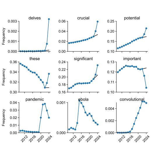
Frequencies of PubMed abstracts containing certain words. Black lines show counterfactual extrapolations from 2021–22 to 2023–24. The first six words are affected by ChatGPT; the last three relate to major events that influenced scientific writing and are shown for comparison. (Credit: Kobak et al., 2024)
That students these days love to use ChatGPT for assistance with reports and other writing tasks is hardly a secret, but in academics it’s becoming ever more prevalent as well. This raises the question of whether ChatGPT-assisted academic writings can be distinguished somehow. According to [Dmitry Kobak] and colleagues this is the case, with a strong sign of ChatGPT use being the presence of a lot of flowery excess vocabulary in the text. As detailed in their prepublication paper, the frequency of certain style words is a remarkable change in the used vocabulary of the published works examined.
For their study they looked at over 14 million biomedical abstracts from 2010 to 2024 obtained via PubMed. These abstracts were then analyzed for word usage and frequency, which shows both natural increases in word frequency (e.g. from the SARS-CoV-2 pandemic and Ebola outbreak), as well as massive spikes in excess vocabulary that coincide with the public availability of ChatGPT and similar LLM-based tools.
In total 774 unique excess words were annotated. Here ‘excess’ means ‘outside of the norm’, following the pattern of ‘excess mortality’ where mortality during one period noticeably deviates from patterns established during previous periods. In this regard the bump in words like respiratory are logical, but the surge in style words like intricate and notably would seem to be due to LLMs having a penchant for such flowery, overly dramatized language.
The researchers have made the analysis code available for those interested in giving it a try on another corpus. The main author also addressed the question of whether ChatGPT might be influencing people to write more like an LLM. At this point it’s still an open question of whether people would be more inclined to use ChatGPT-like vocabulary or actively seek to avoid sounding like an LLM.
After Space Shuttle Atlantis’ drive-by repair of the Hubble Space Telescope (HST) in May of 2009, the end of the STS program meant that the space telescope had to fend for itself with no prospect for any further repair missions. The weakest point turned out to be the gyroscopes, with of the original six only three functioning until May 24th of 2024 when one failed and couldn’t be reset any more. To make the most out of the HST’s remaining lifespan, NASA decided to transition again to single-gyroscope operation, with the most recent imaging results showing that this enables HST to return to its science mission.
Although the HST has operated with a reduced number of gyroscopes before, while awaiting its (much delayed) 2009 Servicing Mission 4, this time around it would appear that no such aid is coming. Although HST is still very much functional even after recently celebrating its 34th year in space, there is a lot of debate about whether another servicing mission could be organized, or whether HST will be deorbited in a number of years. Recently people like [Jared Isaacman] have suggested ideas for an STS servicing mission, with [Jared] even offering to pay for the entire servicing mission out of pocket.
While there is an argument to be made that a Crew Dragon is a poor substitute for a Shuttle with its big cargo bay, airlock and robotic arm, it’s promising to see at least that for now HST can do what it does best with few compromises, while we may just see Servicing Mission 5 happening at some point before that last gyro kicks the bucket.